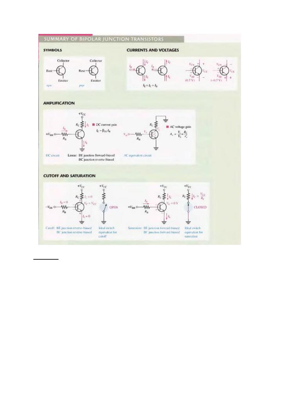
CHAPTER ONE
BIPOLAR JUNCTION TRANSISTORS
Two basic types of transistors are the bipolar junction transistor (BJT), which we will begin to study
in this chapter, and the field-effect transistor (FET), which we will cover in
later chapters. The BJT is used in two broad areas-as a linear amplifier to boost or amplify an
electrical signal and as an electronic switch.
TRANSISTOR STRUCTURE
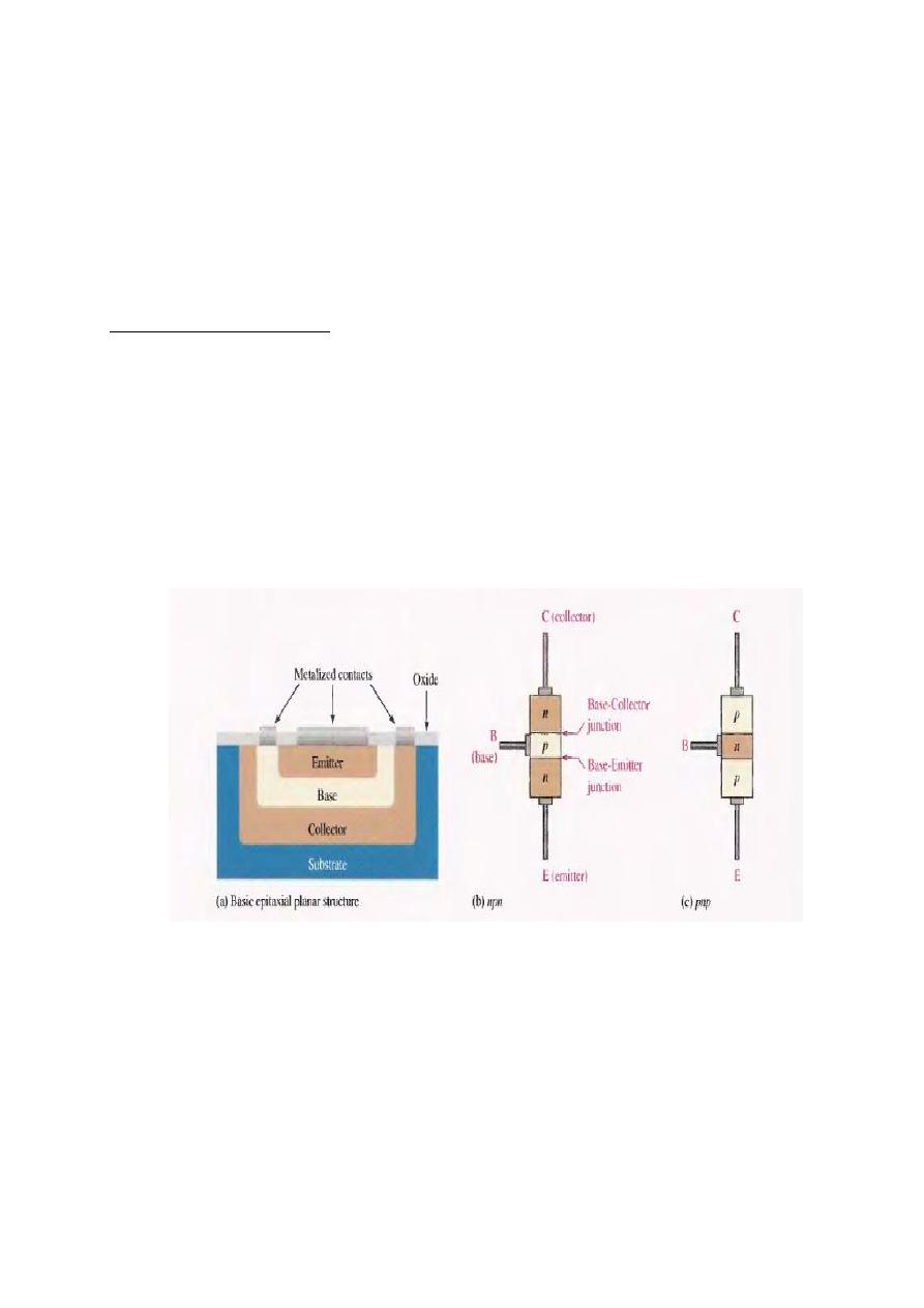
The BJT (bipolar junction transistor) is constructed with three doped semiconductor
regions eparated by two pn junctions, as shown in the epitaxial planar structure in Figure(1-1a). The
three regions are called emitter, base, and collector. Physical representations of the two types of BJTs
are shown in Figure 1-l(b) and (c). One type consists of two n regions separated by a p region (npn),
and the other type consists of two p regions separated by an n region (pnp).
The pn junction joining the base region and the emitter region is called the base-emitter junction. The
pn junction joining the base region and the collector region is called the base-collector junction, as
indicated in Figure 1-1(b). A wire lead connects to each of the three regions, as shown. These leads
are labeled E, B. and C for emitter, base, and collector. Respectively. The base region is lightly doped
and very thin compared to the heavily doped emitter and the moderately doped collector regions.
Figure(1-1): Basic BjT construction.
Figure 1-2 shows the schematic symbols for the npn and pnp bipolar junction transistors. The term
bipolar refers to the use of both holes and electrons as carriers in the transistor structure.
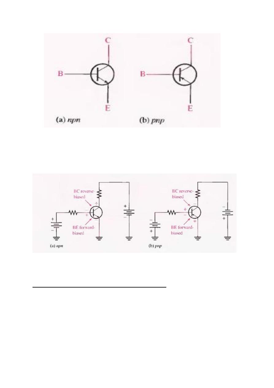
Figure(1-2): Standard BJT (bipolar junction transistor) symbols.
Figure 1-3 shows the proper bias arrangement for both npn and pnp transistors for active operation as
an amplifier. Notice that in both cases the base-emitter (BE) junction is
forward-biased and the base-collector (Be) junction is reverse-biased.
Figure(1-3): Forward-reverse bias of a BJT
TRANSISTOR CHARACTERISTICS AND PARAMETERS.
When a transistor is connected to dc bias voltages, as shown in Figure 1-4 for both npn and pnp types.
V
BB
forward-biases the base-emitter junction, and Vcc reverse-biases the base-collector junction..
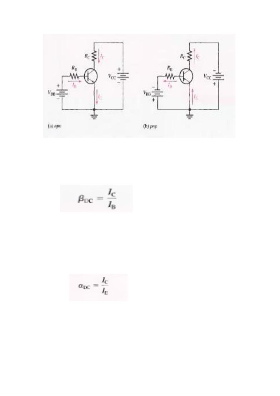
Figure 1-4: Transistor dc bias circuits
The ratio of the dc collector current (I
C
) to the dc base current (l
B
) is the dc beta ({β
DC
),
which is the dc current gain of a transistor.
Typical values of β
DC
range from less than 20 to 200 or higher. β
DC
is usually designated as
an equivalent hybrid (h) parameter, h
FE
, on transistor data sheets.
h
FE
= β
DC
The ratio of the dc collector current (I
C
) to the dc emitter current (I
E
) is the dc
alpha (
α
DC
). The alpha is a less-used parameter than beta in transistor circuits.
Typically, values of
α
DC
range from 0.95 to 0.99 or greater, but
α
DC
is al
ways less than 1.
The reason is that IC is always slightly less than IE by the amount of lB' For example, if IE =
100 mA and I B = I mA, then IC = 99 mA and
α
DC
= 0.99,
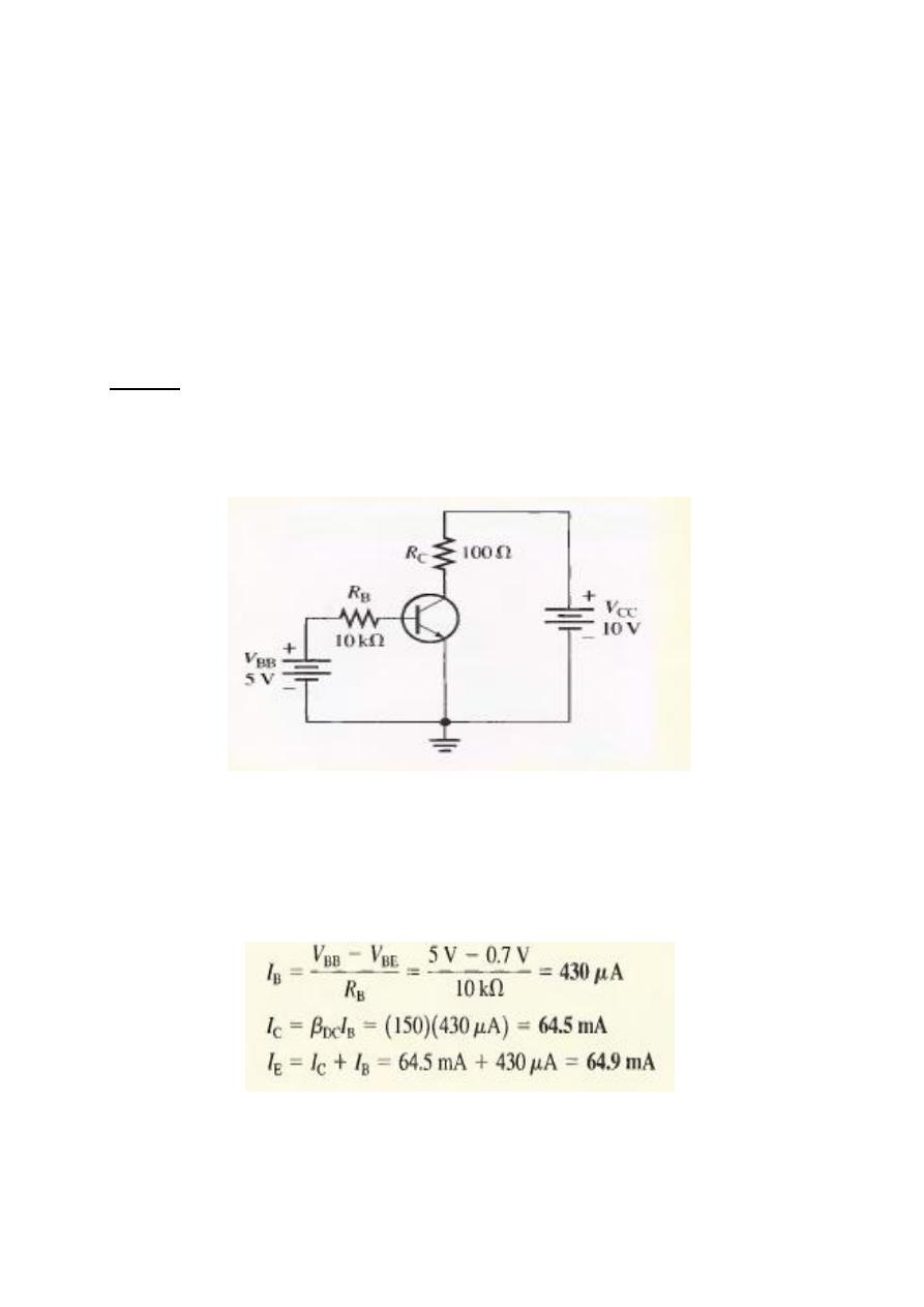
Current and Voltage Analysis
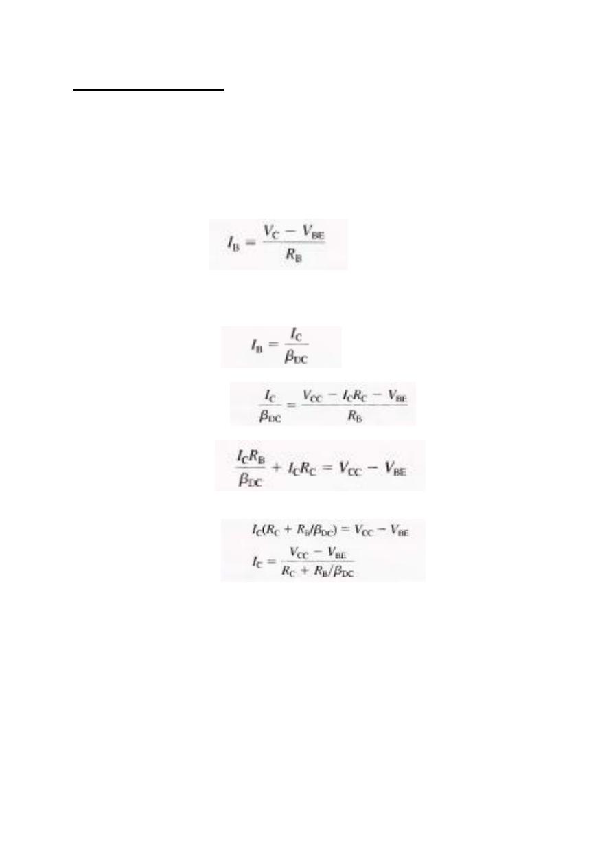
Consider the basic transistor bias circuit configuration in Figure 4-7. Three transistor dc
currents dnd three dc voltages can be identified.
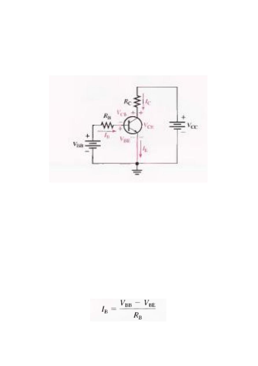
I B : dc base current
IE: dc emitter current
IC: dc collector current
V BE : dc voltage at base with respect to emitter
V CB : dc voltage at collector with respect to base
V CE : dc voltage at collector with respect to emitter
Figure 1-5 : Transistor currents and voltages.
V
BE
== 0.7 V
V
RB
= V
BB
- V
BE
Also, by Ohm's law,
V
RB
= I
B
R
B
Substituting for V RB yields
I
B
R
B
= V
BB
- V
BE
Solving for I B ,
The voltage at the collector with respect to the grounded emitter is
V
CE
= V
CC
- V
RC
Since the drop across Rc is
V
RC
= IcRc
the voltage at the collector can be written as:
V
CE
= V
CC
– I
C
R
C
where Ic = βI
B
The voltage across the reverse-biased collector-base junction is
V
CB
= V
CE
- V
BE
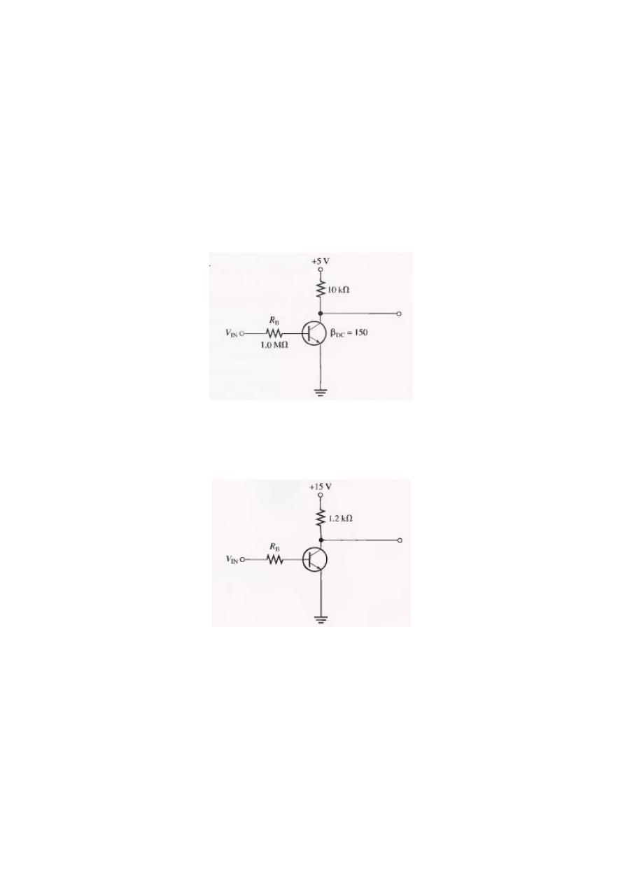
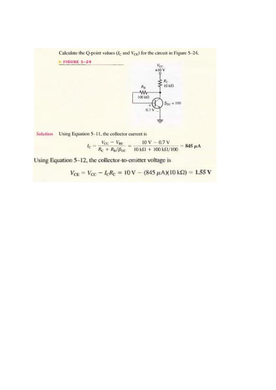
Example
Determine IB, Ic, I
E
, V
BE
' V
CE
, and V
CB
in the circuit of Figure 1-5. The transistor has a
β
DC
= 150.
Figure1-6:
Solution:
V BE= 0.7 V. Calculate the base, collector, and emitter Cllirents as follows:
Solve for V eE and VeB'
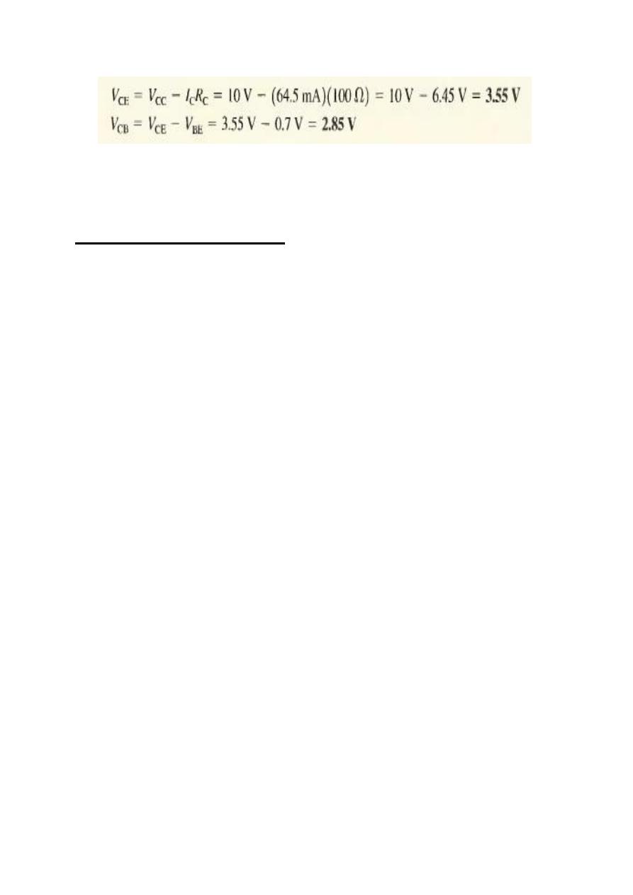
Since the collector is at a higher voltage than the base, the collector-base junction is reverse-
biased.
Collector Characteristic Curves
Using a circuit like that shown in Figure 1-7(a), you can generate a set of collector
characteristic curves that show how the collector curreent, Ic varies with the collector-to-
emitter voltage, V
CE
' for specified values of base current, lB' Notice in the circuit diagram
that both V BB and V cc are variable sources of voltage.
Assume that V BB is set to produce a certain value of I B and V cc is zero. For this condi-
tion, both the base-emitter junction and the base-collector junction are forward-biased
because the base is at approximately 0.7 V while the emitter and the collector are at 0 V.
The base currenent is through the base-emitter junction because of the low impedance path to
ground and, therefore, Ic is zero. When both junctions are forward-biased, the transistor is
in the saturation region of its operation.
As V cc is increased, V CE increases gradually as the collector current increases. This is in-
dicated by the portion of the characteristic curve between points A and B in Figure 1-7(b).
Ic increases as V cc is increased because V CE remains less than 0.7 V due to the forward-
biased base-collector junction.
Ideally, when V CE exceeds 0.7 V, the base-collector junction becomes reverse-biased and
the transistor goes into the active or linear region of its operation. Once the base-collector
junction is reverse-biased, Ic levels off and remains essentially constant for a given value of
I
B
as V CE continues to increase. Actually, Ic increases very slightly as V CE increases due
to widening of the base-collector depletion region. This results in fewer holes for
recombination in the base region which effectively causes a slight increase in (3oc. This is
shown by the portion of the characteristic curve between points B and C in Figure 1-7(b). For
this portion of the characteristic curve, the value of Ic is determined only by the relationship
expressed as Ic = β
DC
I B .
When V CE reaches a sufficiently high voltage, the reverse-biased base-collector junction
goes into breakdown; and the collector current increases rapidly as indicated by the part of
the curve to the right of point C in Figure 1-7(b). A transistor should never be operated in
this breakdown region.
A family of collector characteristic curves is produced when Ic versus V CE is plotted for
severa] values ofI B , as illustrated in Figure1-7(c). When I B = 0, the transistor is in the
cutoff region although there is a very small collector leakage CUlTent as indicated. The
amount of collector leakage CUlTent for I B = 0 is exaggerated on the graph for illustration.
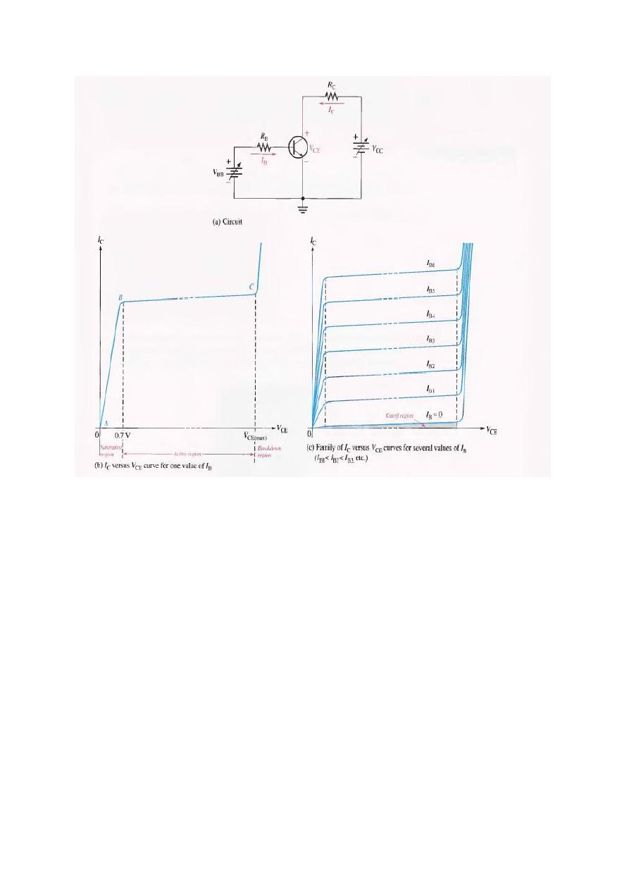
Figure1-7: Collector characteristic curves.
Example:
Sketch an ideal family of collector curves for the circuit in Figure 1-8 for I B = 5 μA
to 25 μA in 5 μA increments. Assume {β
DC
= 100 and that V CE does not exceed
breakdown..
Solution:
Using the relationship Ic = β
DC
IB values of Ic are calculated and tabulated in Table 1-
1. The resulting curves are plotted in Figure 1-9. These are ideal curves because the
slight increase in Ic for a given value of I B as V CE increases in the active region is
neglected.
Table 1-1
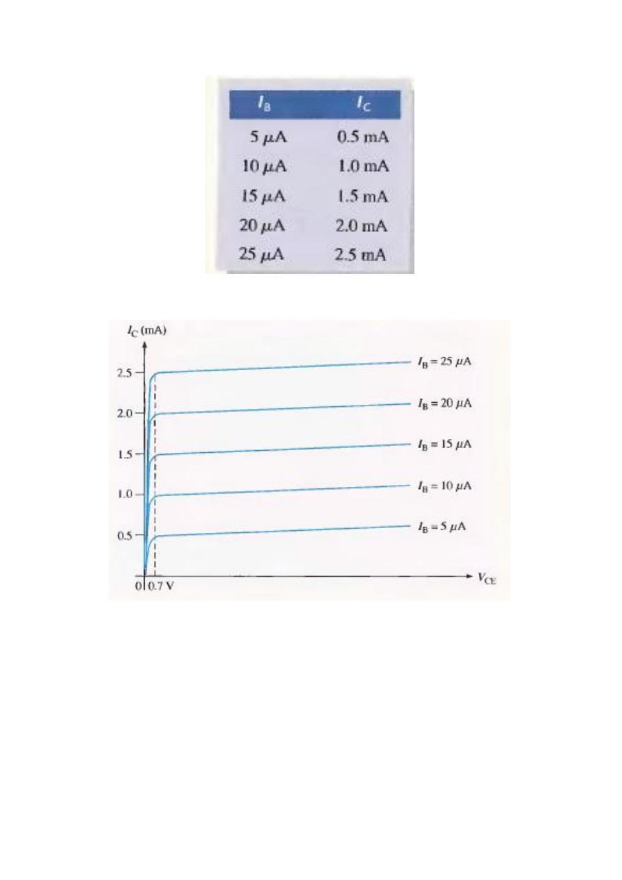
Figure1-9
Cutoff:
As previously mentioned. when I B = 0, the transistor is in the cutoff region of its
operation. This is shown in Figure 1-10 with the base lead open. resulting in a base
current of zero. Under this condition, there is a very small amount of collector leakage
current. I
CEO'
due mainly to thermally produced carriers. Because I
CEO
is extremely
small. it will usually be neglected in circuit analysis so that V
CE
= V cc . In cutoff,
both the base-emitter and the base-
collector junctions are reverse-biased.
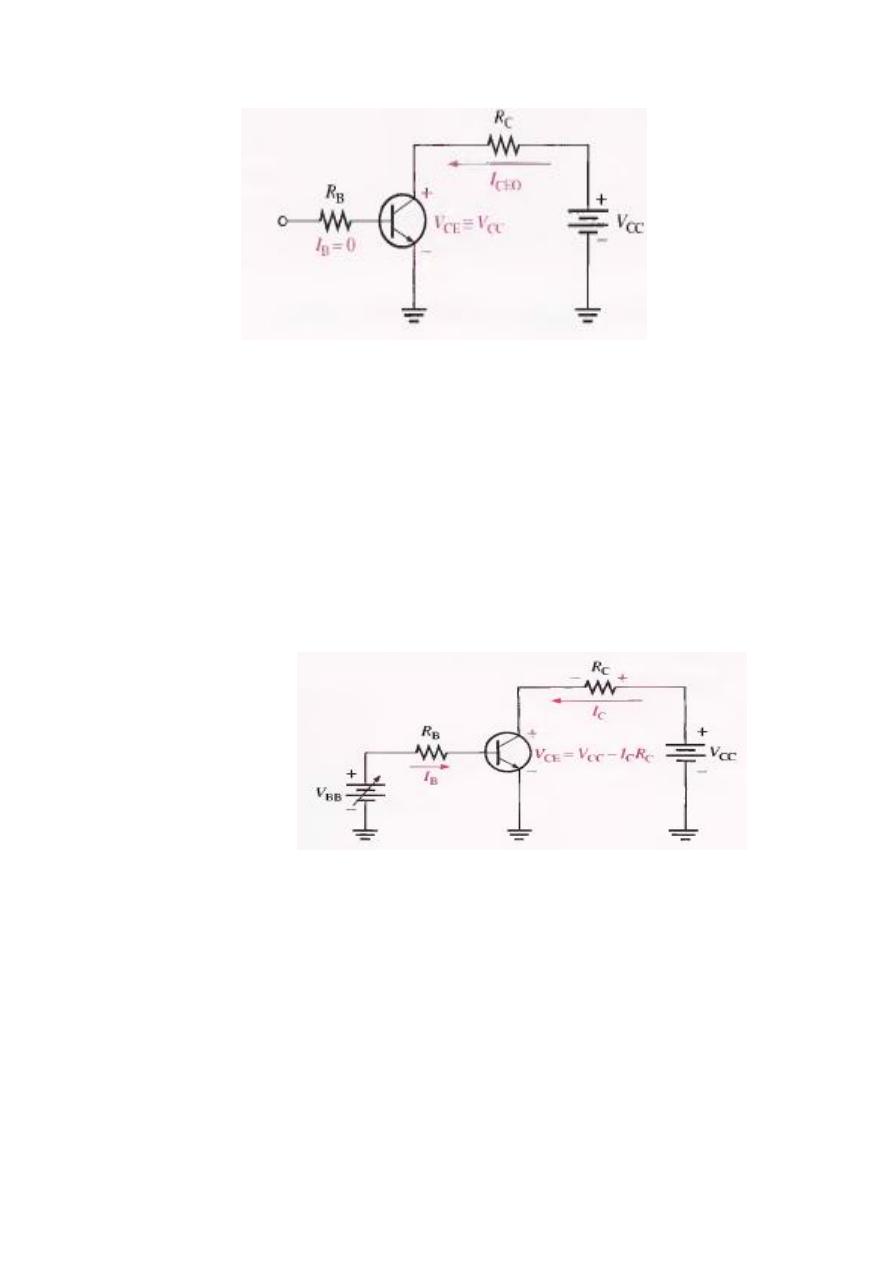
Figure1-10:
Cutoff: Collector leakage current (tcw) is extremely small and is
usuallyneglected. Base-emitter and base-collector junctions are reverse-biased.
Saturation:
When the base-emitter junction becomes forward-biased and the base current is
increased, the collector current also increases (lc = β
DC
I
B
) and V
CE
decreases as a
result of more drop across the collector resistor (VCE = V cc - IcRc). This is
illustrated in Figure 1-11. When V
CE
reaches its saturation value. V
CE(sat)
, the base-
collector junction becomes forward-biased and Ic can increase no further even with a
continued increase in I
B
. At the point of saturation, the relation Ic = β
DC
I
B
is no
longer valid. V
CE(sat)
for a transistor occurs somewhere below the knee of the collector
curves, and it is usually only a few tenths of a volt for silicon transistors.
FIGURE 1-11
DC load line:
Cutoff and saturation can be illustrated in relation to the collector characteristic curves
by the use of a load line. Figure 4-12 Shows a de load line drawn on a family of
curves connecting the cutoff point and the saturation point. The bottom of the load
line is at ideal cutoff where Ic = 0 and V CE = Vcc. The top of the load line is at
saturation where Ic = IC(sat) and V CE = VCE(sat)- In between cutoff and saturation
along the load line is the active region of the transistor's operation.
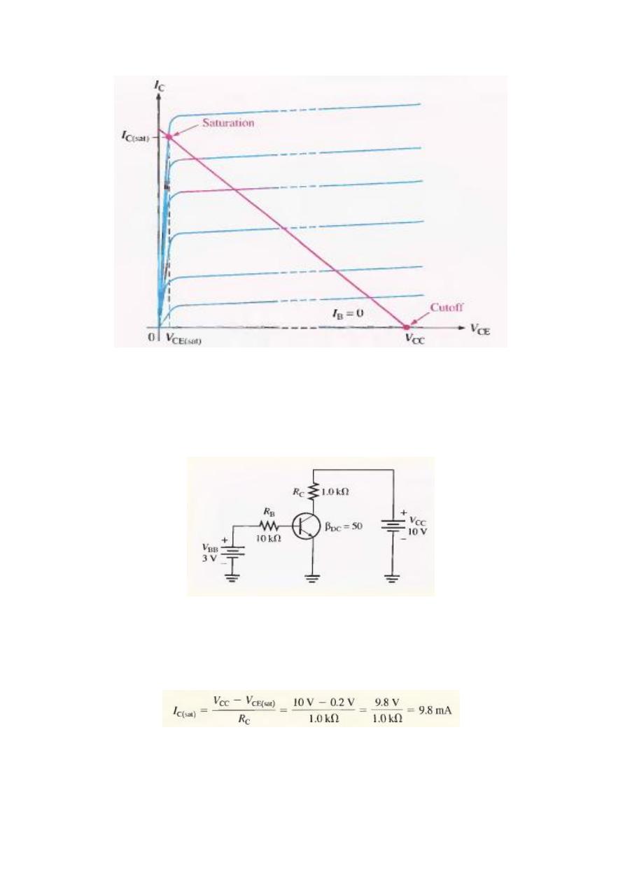
Figure1-12
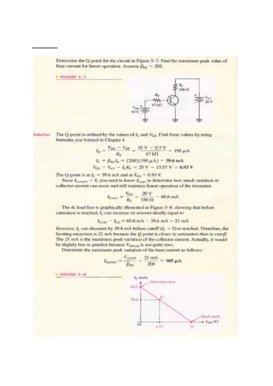
Example:
Determine whether or not the transistor in Figure 4-13 is in saturation. Assume
VCECsat = 0.2 V.
Figure1-13
Solution
First, determine I
CE(sat)
:
Now. see if I B is large enough to produce Ic(sat).
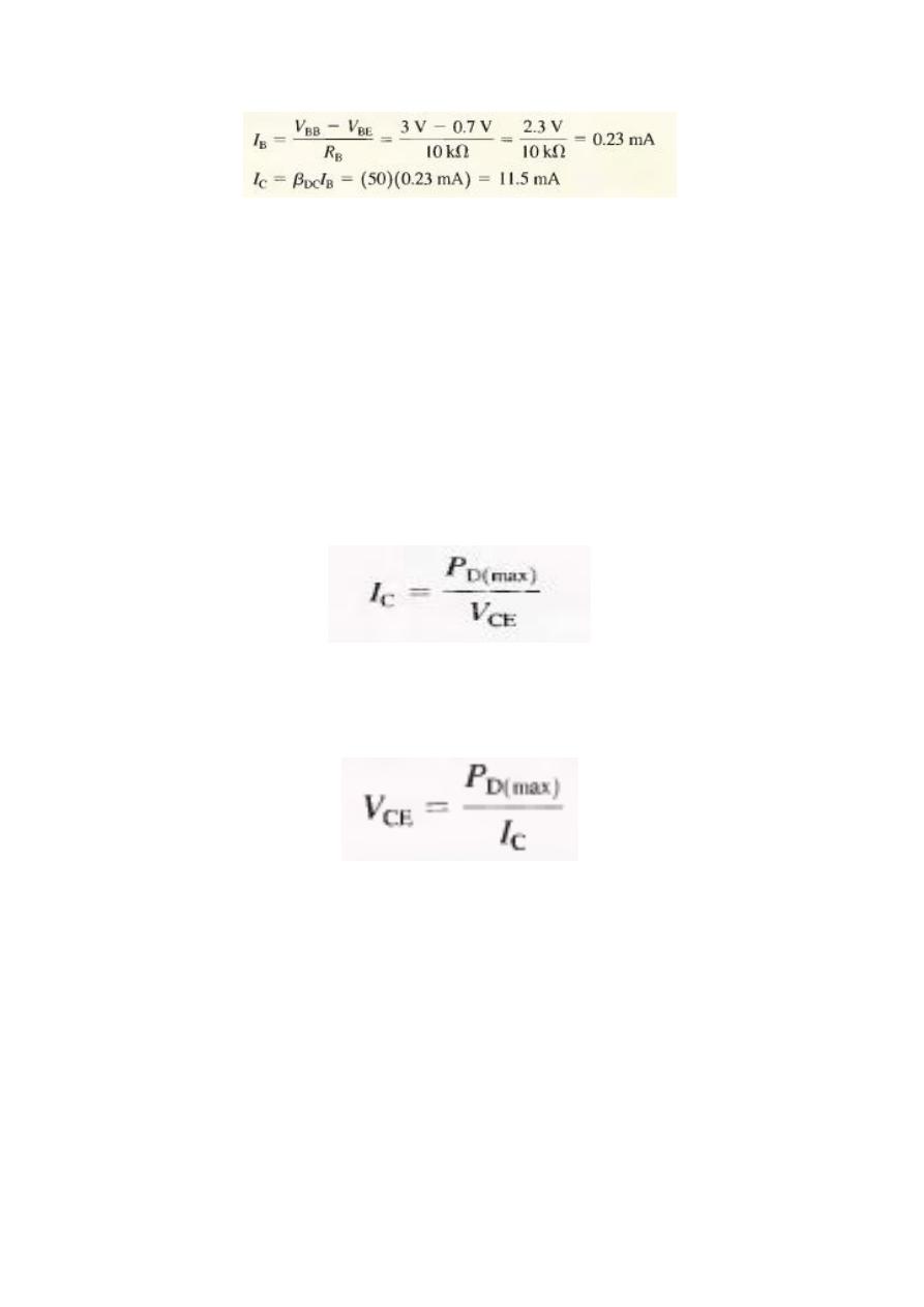
This shows that with the specified β
DC
, this base current is capable of producing an Ic
greater than IC(sat). Therefore, the transistor is saturated, and the collector current
value of 11.5 mA is never reached. If you further increase IB' the collector current
remains at its saturation value.
Maximum Transistor Ratings:
A transistor, like any other electronic device, has limitations on its operation. These
limitations are stated in the form of maximum ratings and are normally specified on
the manufacturer's data sheet. Typically, maximum ratings are given for collector-to-
base voltage. collector-to-emitter voltage. emitter-to-base voltage. collector current,
and power dissipation. The product of V CE and Ic must not exceed the maximum
power dissipation. Both V CE and Ic cannot be maximum at the same time. If V CE is
maximum. Ic can be calculated as:
If Ic is maximum, V CE can be calculated by rearranging the above Equation as
follows:
For any given transistor, a maximum power dissipation curve can be plotted on the
collector characteristic curves, as shown in Figure 1-14(a). These values are tabulated
in Figure 1-14(b). Assume PO(max) is 500 mW, VCE(max) is 20 V, and IC(max) is
50 mA. The curve shows that this particular transistor cannot be operated in the
shaded portion of the graph. IC(max) is the limiting rating between points A and B,
POrmax) is the limiting rating between points Band C, and VCE(max) is the limiting
rating between points C and D.
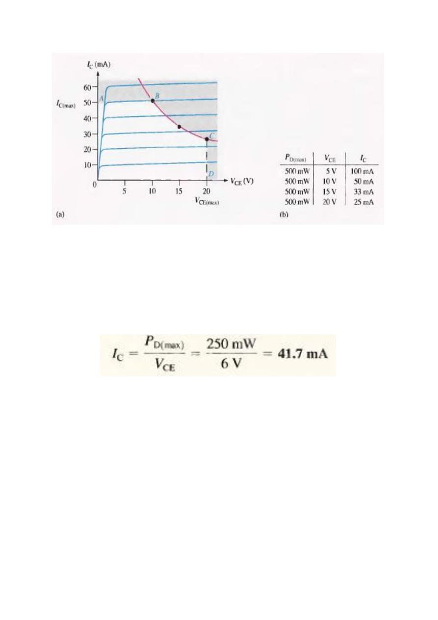
Figure1-14
Example:
A certain transistor is to be operated with V CE = 6 V. If its maximum Power rating
is 250 mW. what is the most collector cunent that it can handle?
Solution
Remember that this is not necessarily the maximum Ic. The transistor can handle more
collector current if V CE is reduced, as long as PD(max) is not exceeded.
Example:
The transistor in Figure 1-15 has the following maximum ratings: PD(max) = 800
mW. V
CEmax
= 15 V, and I
C
(max) = 100 mA. Determine the maximum value to which
V
CC
can be adjusted without exceeding a rating. Which rating would be exceeded
first?
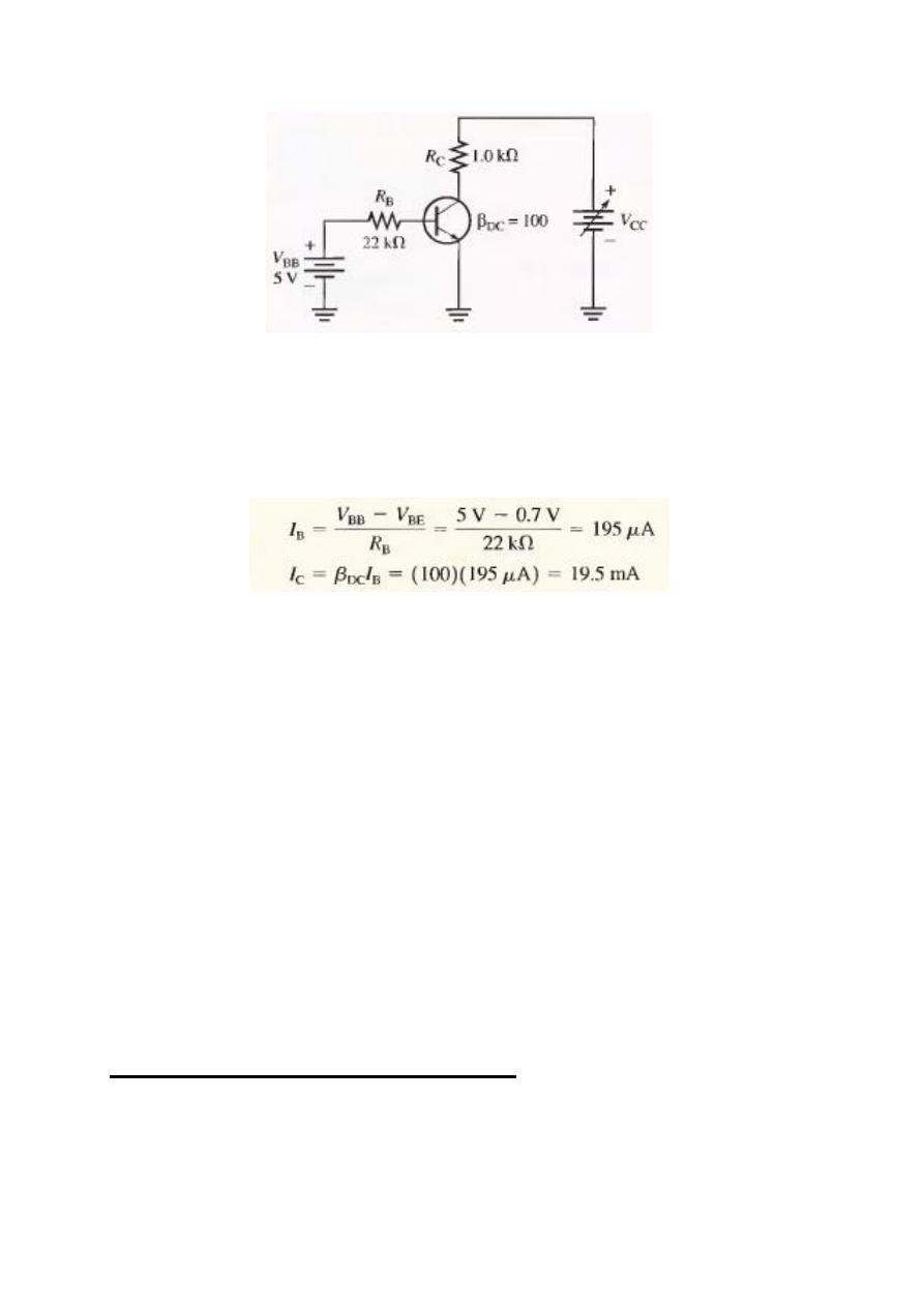
Figure1-15
Solution
First find I B so that you can determine I
C
.
Ie is much less than IC\max) and will not change with Vee. It is determined only by
I
B
and β
DC
. The voltage drop across Rc is
V
RC
= IcRc = (19.5 mA)(l.O kΩ) = 19.5 V
Now you can determine the value of Vcc when V
CE
= V
CEmax
= 15 V.
V
Rc
= Vcc- V
CE
So.
Vcc(max) = V
CE
(max) + V
Rc
= 15 V + 19.5 V = 34.5 V
V cc can be increased to 34.5 V, under the existing conditions, before V
CEmax
is
exceeded. However, at this point it is not known whether or not PD(maxl has been
exceeded.
P
D
= VCE(max) Ic= (15 V)(19.5 mA) = 293 mW
Since PD(max) is 800 mW, it is not exceeded when Vcc = 34.5 V. So, VCE(max) =
15 V is the limiting rating in this case. If the base current is removed causing the
transistor to turn off, V
CEmax
will be exceeded first because the entire supply voltage,
Vcc will be dropped across the transistor.
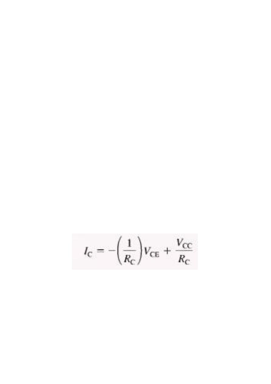
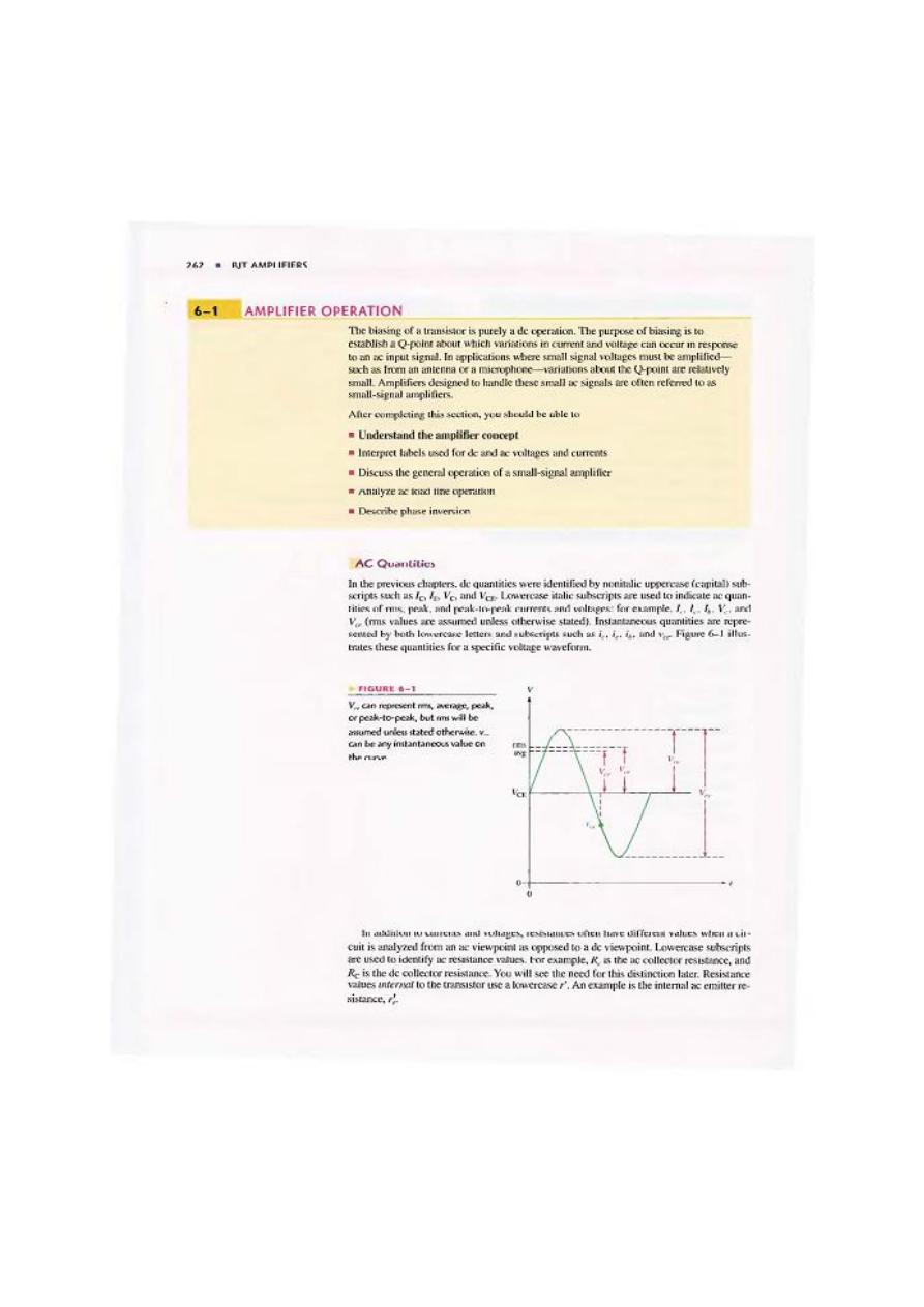
THE TRANSISTOR AS AN AMPLIFIER
As you have learned, a transistor amplifies cunent because the collector current is
equal to the base CUITent multiplied by the CUlTent gain, (3. The base current in a
transistor is very small compared to the collector and emitter currents. Because of this,
the collector current is approximately equal to the emitter current.
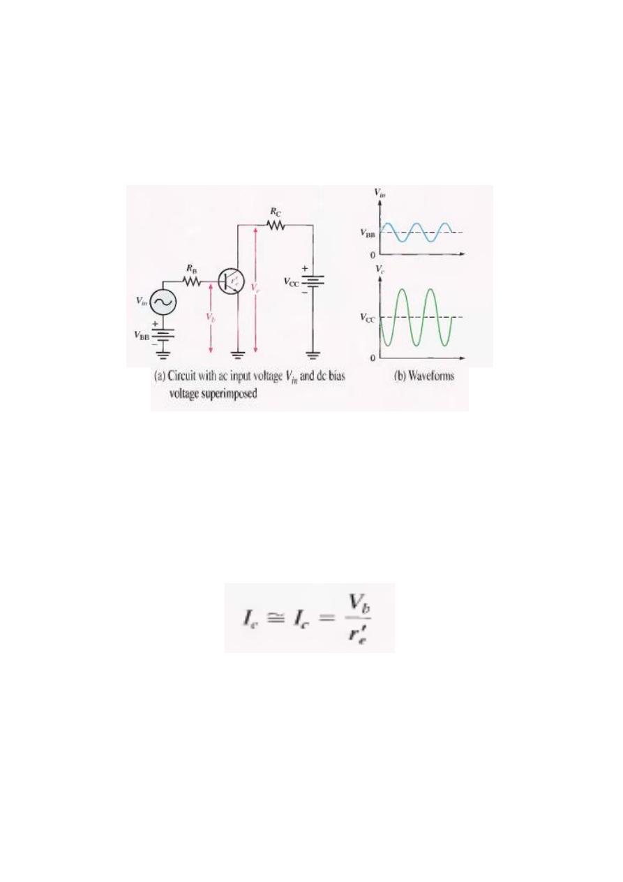
With this in mind, let's look at the circuit in Figure 1-16(a). An ac voltage, Vin, is
superimsoed on the dc bias voltage VBB by connecting them in series with the base
resistor, R
B
, as shown. The dc bias voltage Vcc is connected to the collector through
the collector resistor, Rc.
Figure 1-16 Basic transistor amplifier circuit.
The ac input voltage produces an ac base current, which results in a much larger ac
collector current. The ac collector current produces an ac voltage across Rc, thus
producing an amplified. but inverted, reproduction of the ac input voltage in the active
region of operation, as illustrated in Figure 1-16(b).
The forward-biased base-emitter junction presents a very low resistance to the ac
signal This internal ac emitter resistance is designated r. In Figure 1-16(a), the ac
emitter current is
The ac collector voltage. V c , equaJs the ac voJtage drop acros Rc.
V c = Ic.Rc
Since Ic = Ie, the ac collector voltage is
V e = IeRe
Vb can be considered the transistor ac input voltage where Vb = V in – I
b
R
B
.,
Vc can be considered the transistor ac output voltage. The ratio of Vc to Vb is the ac
voltage gain, Av, of the transistor circuit.
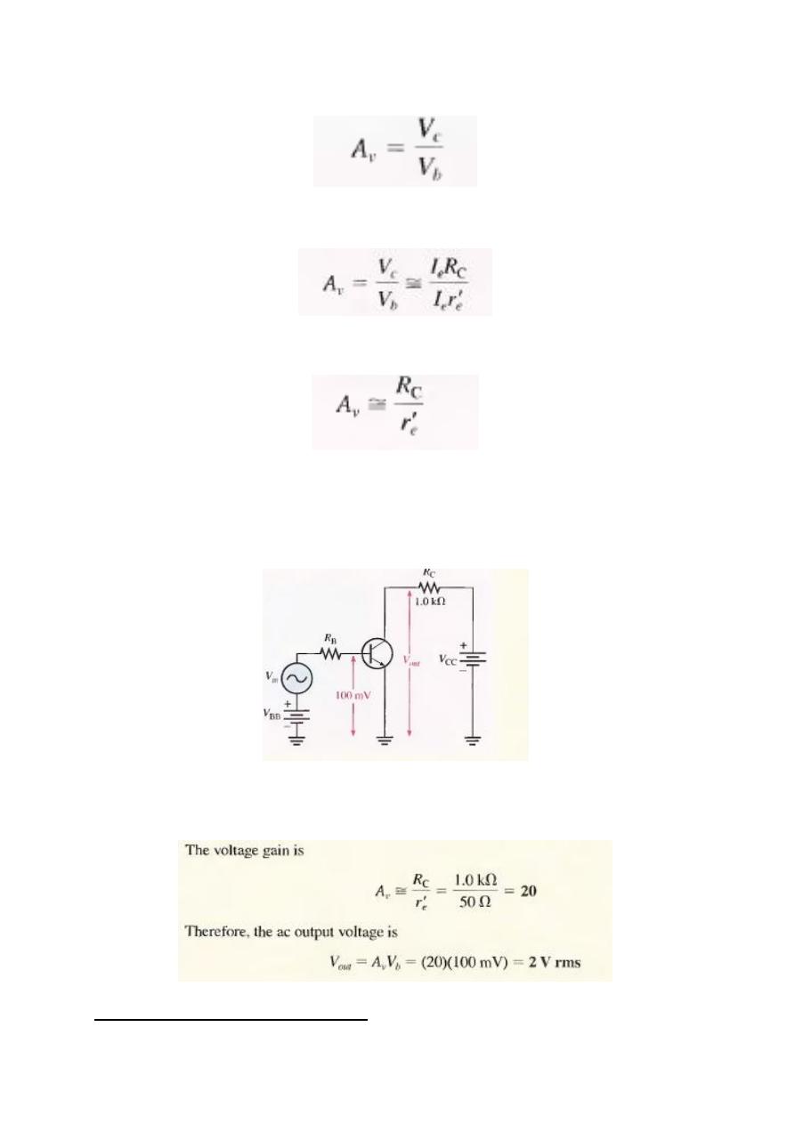
Substituting IeRc for Vc and
Ie r
e
for Vb yields
The Ie terms cancel; therefore,
Since Rc is always considerably larger in value than re, the output voltage is always
greater than the input voltage. Various types of amplifiers are covered in detail in later
chapters.
Example: Determine the voltage gain and the ac output voltage in Figure 1-17 if re =
50 Ω.
Figure 1-17
Solution
THE TRANSISTOR AS A SWITCH
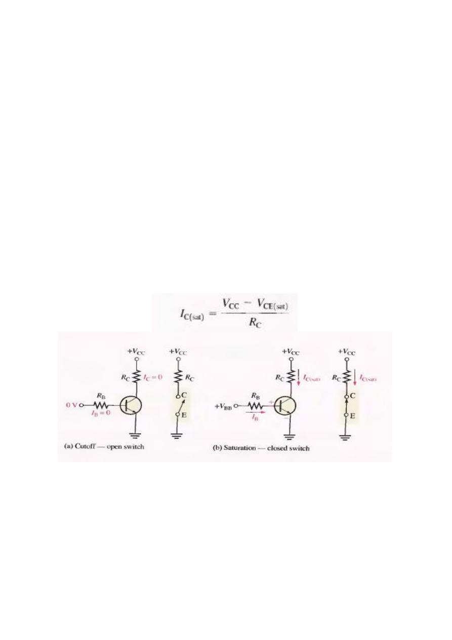
Figure 1-18 illustrates the basic operation of the transistor as a switching device. In
part (a). the transistor is in the cutoff region because the base-emitter junction is not
forward-biased. In this condition, there is, ideally, an open between collector and
emitter, as indicated by the switch equivalent. In part (b), the transistor is in the
saturation region because the base-emitter junction and the base-collector junction are
forward-biased and the base current is made large enough to cause the collector
current to reach its saturation value. In this condition, there is, ideally, a short
between collector and emitter, as indicated by the switch equivalent. Actually, a
voltage drop of up to a few tenths of a volt normally occurs, which is the saturation
voltage. V CE (sat).
Conditions in Cutoff: As mentioned before, a transistor is in the cutoff region when
the base-emitter junction is not forward-biased. Neglecting leakage current, all of the
currents are zero, and V CE is equal to V cc.
VCE(cutoff) = V cc
Conditions in Saturation: As you have learned. when the base-emitter junction is
forward-biased and there is enough base current to produce a maximum col1ector
current. the transistor is saturated. The formula for collector saturation current is:
figure1-17: Ideal switching action of a transistor.
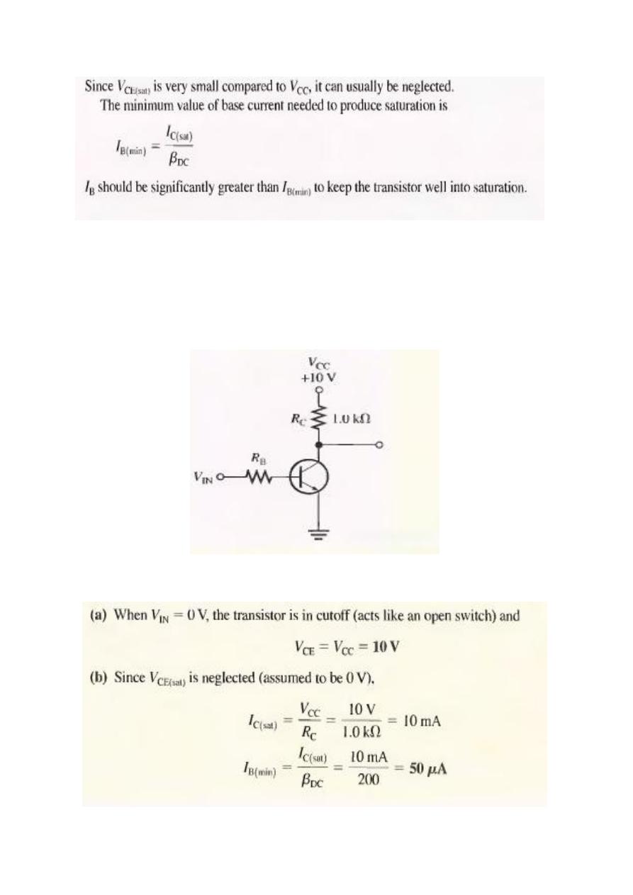
Example:
(a) For the transistor circuit in Figure 1-18, what is V CE when V
1N
= 0 V?
(b) What minimum value of I
B
is required to saturate this transistor if β
DC
is 200?
Neglect VCE(sat)"
(c) Calculate the maximum value of R
when VIN = 5 V.
Figure1-18
Solution
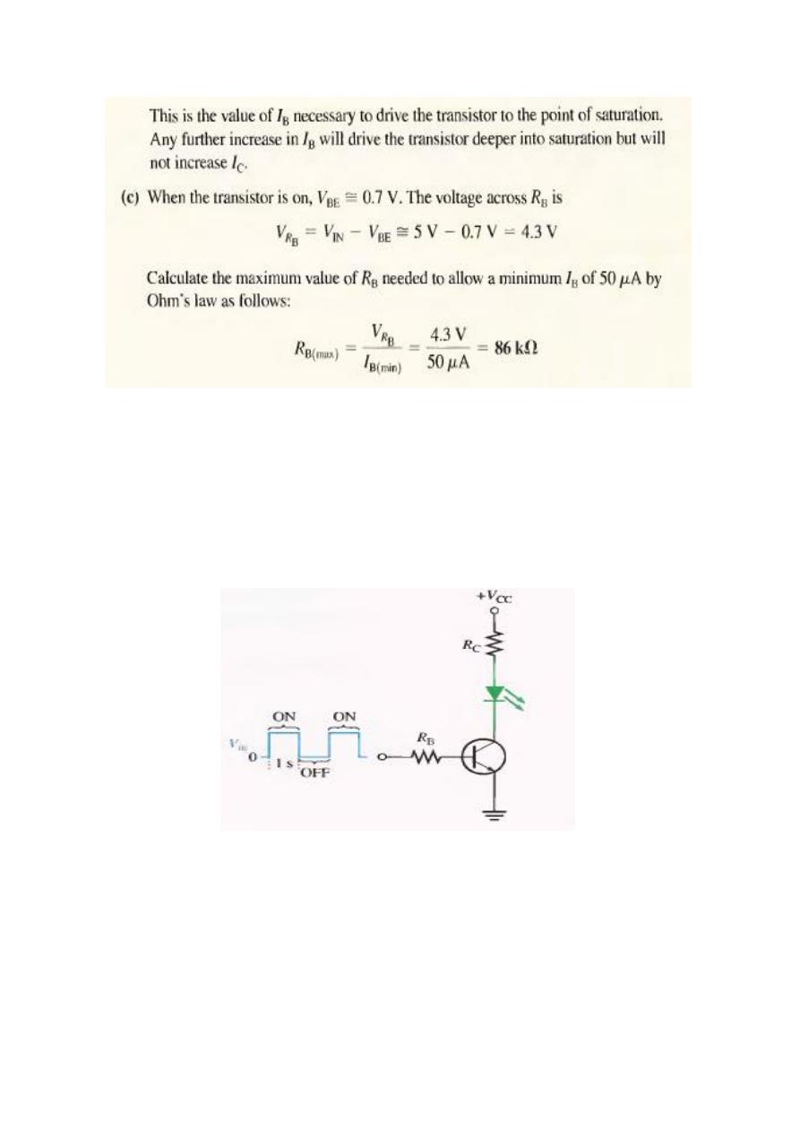
A Simple Application of a Transistor Switch
The transistor in Figure 1-19 is used as a switch to turn the LED on and off. For
example. a square wave input voltage with a period of 2 s is applied to the input as
indicated. When the square wave is at 0 V, the transistor is in cutoff; and since there is
no collector current. the LED does not emit light. When the square wave goes to its
high level, the transistor saturates. This forward-biases the LED, and the resulting
collector current through the LED causes it to emit light. Thus, the LED is on for I s
and off for 1 s.
Figure1-19
Self Test
3. For operation as an amplifier, the base of an npn transistor must be
(a) positive with respect to the emitter (b) negative with respect to the emitter
(c) positive with respect to the collector (d) 0 V
4. The emitter current is always
(a) greater than the base current
(c) greater than the collector current
5. The {3DC of a transistor is its
(a) current gain (bl voltage gain (c) power gain
6. If Ie is 50 times larger than IE' then (3DC is
(b) less than the collector current
(d) answers (a) and (c)
(d) internal resistance
(a) 0.02
(b) 100
(c) 50
(d) 500

7. The approximate voltage across the forward-biased base-emitter junction of a silicon BIT is
(a) 0 V
(b) 0_7 V
(c) 0.3 V
(d) V BE
8. The bias condition for a transistor to be used as a linear amplifier is called
(a) forward-reverse (b) forward-forward (e) reverse-reverse (d) collector bias
9. If the output of a transistor amplifier is 5 V rms and the input is 100 m V rms, the voltage
gain is
(a) 5
(b) 500
(e) 50
(d) 100
10. When operated in cutoff and saturation, the transistor acts like a
(a) linear amplifier (b) switch (c) variable capacitor (d) variable resistor
11. In cutoff, V CE is
(a) 0 V (b) mtmmum
(d) equal to V ec (e) answers (a) and (b)
12. In saturation, V eE is
(a) 0_7 V (b) equal to V cc (e) mllllmum
13. To saturate a BIT,
(a) IE = losau (b) IE> losat/{3Dc
(e) V ee must be at least 10 V (d) the emitter must be grounded
14. Once in saturation, a further increase in base current will
(a) cause the collector current to increase
(b) not affect the collector current
(el maxtmum
m answers (c) and (d)
(d) maximum
(c) cause the collector current to decrease
(d) tum the transistor off
15. If the base-emitter junction is open, the collector voltage is
(a) V cc (b) 0 V (c) floating (d) 0.2 V
PROBLEMS
Basic Transistor Operation
3. Why is the base current in a transistor so much less than the collector current?
4. In a certain transistor circuit, the base current is 2 percent of the 30 mA emitter current.
Determine the collector current
Transistor Characteristics and Parameters
7. What is the α
DC
when Ic = 8.23 mA and IE = 8_69 mA?
8. A certain transistor has an Ic = 25 mA and an I B = 200 μ.A. Determine the β
DC
.
9. What is the βDC of a transistor if Ic = 20.5 mA and IE = 20.3 mA?
10. What is the α
DC
if Ic = 5.35 mA and I B = 50 μ.A?
11. A certain transistor exhibits an α
DC
of 0.96 Detemine Ic when IE = 9.35 mA.
12. A base current of 50μA is applied to the transistor in Figure 4-45. and a voltage of 5 V is
dropped across Rc. Determine the β
DC
of the transistor.
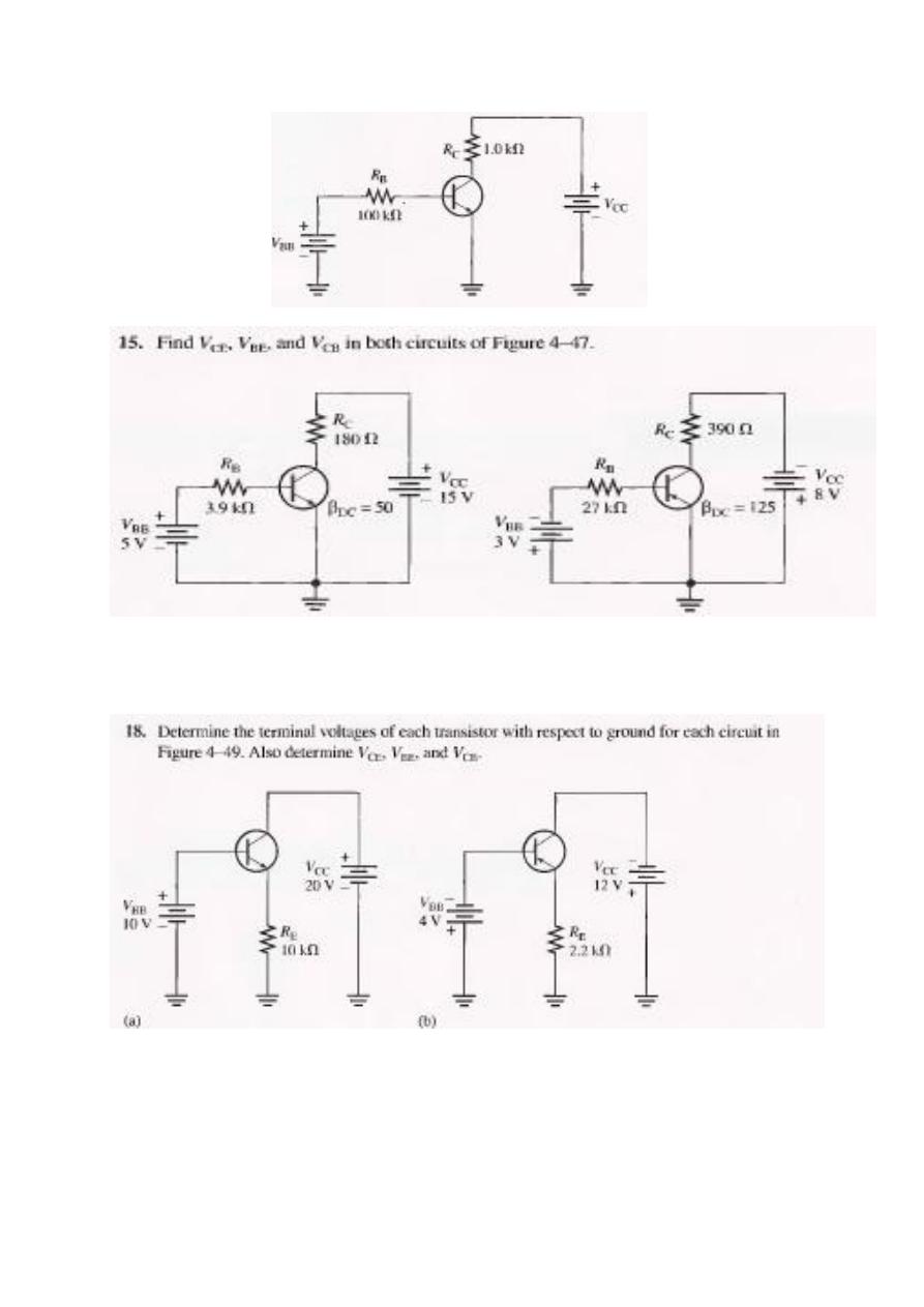
Figure 4-47
Figure 4-49
19. If the β
DC
in Figure 4-49(a) changes from 100 to 150 due to a temperature increase, what is the
change in collector current?
20. A certain transistor is to be operated at a collector current of 50 mA. How high can V CE
gowithout exceeding a PD(max) of 1.2 W?
21. The power dissipation derating factor for a certain transistor is I mW/C The P
D
(max) is 0.5 W at
25°C. What is P
D
(max) at 100°C?
The Transistor as an Amplifier
22. A transistor amplifier has a voltage gain of 50. What is the output voltage when the input
voltage is 1 00 mV?
23. To achieve m output of 10 V with an input of 300 mV, what voltage gain is required?
24. A 50 mV signal is applied to the base of a properly biased transistor with r;, = 10Ω and
Rc = 560Ω. Determine the signal voltage at the collector.
The Transistor as a Switch
25. Determine I
Csat
for the transistor in Figure 4-50. What is the value of I
B
necessary to produce
saturation? What minimum value of V
IN
is necessary for saturation? Assume VCE(Sat) = 0 v.
Figure4-50
26. The transistor in Figure 4-51 has a β
DC
of 50. Determine the value of R
B
required to ensure
saturation when V
IN
is 5 V. What must V
IN
be to cut off the transistor? Assume
V
CE(sat
) = 0 v.
Figure4-51
CHAPTER TWO
Transistor Bias Circuits
DC Bias
Bias establishes the de operating point for proper linear operation of an amplifier. If
an amplifier is not biased with correct dc voltages on the input and output. it can go
into saturation or cutoff when an input signal is applied. Figure 2-1 shows the effects
of proper and improper dc biasing of an inverting amplifier.
Figure2-1:
Examples of linear and nonlinear operation of an inverting amplifier
.
Graphical Analysis: The transistor in Figure 2-2(a) is biased with variable voltages
Vcc and V BB to obtain certain values of IB, Ic, IE, and VCE ' The collector
characteristic curves for this particular transistor are shown in Figure 2-2(b); we will
use these curves to graphically illustrate the effects of dc bias.
Figure2-2:
A dc-biased transistor circuit with variable bias voltages (V BB and V cc ) for
generating the collector characteristic curves shown in part (b).
In Figure 2-3, we assign three values to I
B
and observe what happens to Ic and VCE ' First.
V
BB
is adjusted to produce an IB of 200 μA, as shown in Figure 2-3(a). Since Ic = β
DC
I
B
,
the collector current is 20 mA, as indicated, and V CE = Vcc - IcRc = 10 V - (20 mA)(220Ω
= 10 V - 4.-1 V = 5.6 V
This Q-point is shown on the graph of Figure 2-3(a) as Q,.
Next, as shown in Figure 2-3(b), V BB is increased to produce an I
B
of 300 μA and an Ic
of 30 mA.
V CE = lOV - (30 mA)(220 Ω) = 10V – 6.6 V = 3.4 V
The Q-point for this condition is indicated by Q2 on the graph.
Finally. as in Figure 2-3(c), V BB is increased to give an I B of 400 μ A and an Ic of 40 mA.
V CE = 10 V - (40 mA)(220 Q) = 10 V - 8.8 V = 1.2 V
Q3 is the corresponding Q-point on the graph.
DC Load Line: Notice that when I B increases, Ic increases and V CE decreases. When I B
decreases, Ic decreases and V CE increases. As V BB is adjusted up or down, the dc
operating point of the transistor moves along a sloping straight line, called the dc load line,
connecting each separate Q-point. At any point along the line, values of IB, Ic, and V CE can
be picked off the graph, as shown in Figure 2-4.
The dc load line intersects the V CE axis at 10 V. the point where V CE = V cc . This is the
transistor cutoff point because I B and Ic are zero (ideally). Actually. there is a small leak-
age current, I
CBO
, at cutoff as indicated, and therefore V CE is slightly less than 10 V but
normally this can be neglected.
The dc load line intersects the Ic axis at 45.5 mA ideally. This is the transistor saturation
point because Ic is maximum at the point where V CE = 0 V and Ic = Vcc/Rc.
Actually, there is a small voltage (VCE(sat)) across the transistor, and (Icsat) is slightly
less than 45.5 mA, as indicated in Figure 2-4. Note that Kirchhoff's voltage law applied
around the collector loop gives
V cc - IcRc - V CE = 0
This results in a straight line equation for the load line of the form y = mX + b as follows:
where – 1/Rc is the slope and Vcc/R c is the y-axis intercept point.
Linear Operation: The region along the load line including all points between saturation
and cutoff is generally known as the linear region of the transistor's operation. As long as the
transistor is operated in this region, the output voltage is ideally a linear reproduction of the input.
Figure 2-5 shows an example of the linear operation of a transistor.
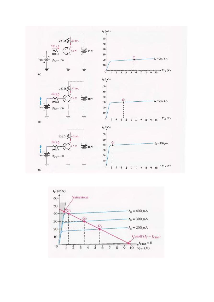
Figure2-3: Illustration of Q-point adjustment.
Figure2-4: DC load line.
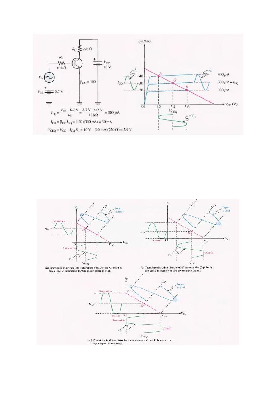
Figure2-5: Variations in collector current and collector-to-emitter voltage as a result of a
variation in base current. Notice that ac quantities are indicated by lowercase italic subscripts.
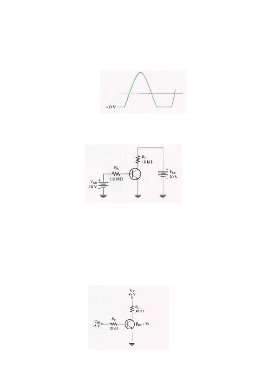
Waveform Distortion As previously mentioned, under certain input signal conditions the location of
the Q-point on the load line can cause one peak of the V ce waveform to be limited or clipped, as
shown in parts (a) and (b) of Figure 2-6. In each case the input signal is too large for the Q-point
location and is driving the transistor into cutoff or saturation during a portion of the input cycle. When
both peaks are limited as in Figure 2-6( c), the transistor is being driven into both saturation and
cutoff by an excessively large input signal. When only the positive peak is limited, the transistor is
being driven into cutoff but not saturation. When only the negative peak is limited, the transistor is
being driven into saturation but not cutoff.
Figure2-6
Example
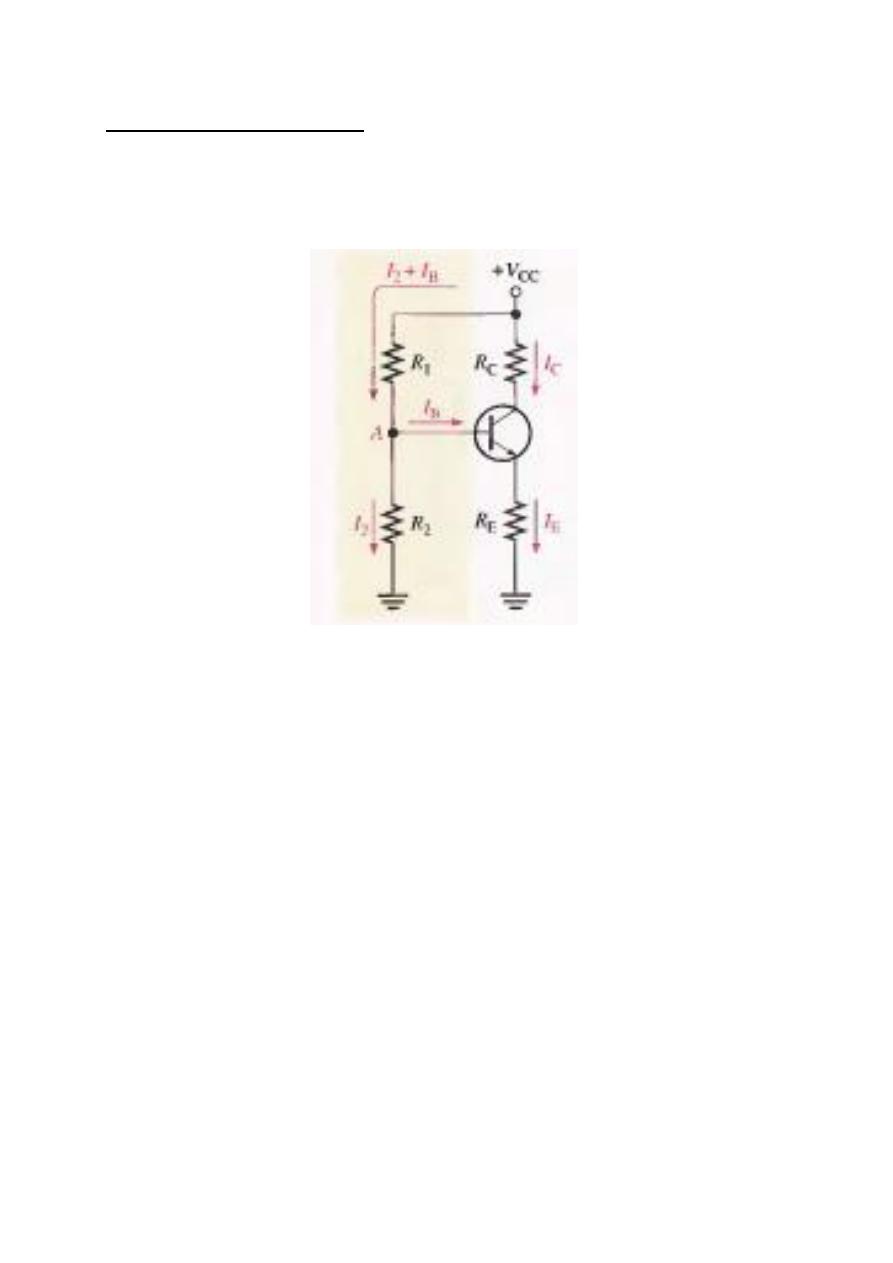
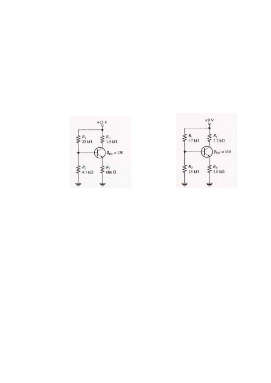
VOLTAGE-DIVIDER BIAS
A de bias voltage at the base of the transistor can be developed by a resistive voltage-
divider that consists of Rl and R2, as shown in Figure 2-7. V cc is the dc collector supply
voltage. Two current paths are between point A and ground: one through R2 and the other
through the base-emitter junction of the transistor and R
E
.
Figure2-7: Voltage-divider bias.
Input Resistance at the Transistor Base
To develop a formula for the dc input resistance at the base of a transistor, we will use the
diagram in Figure 2-8 V
IN
is applied between base and ground, and I
IN
is the current into
the base as shown. By Ohm's law,
R
IN
(base) = V
IN
/ I
IN
Kirchhoff's voltage law applied around the base-emitter circuit yields
V IN = V BE + I
E
R
E
With the assumption that V BE « I
E
R
E
, the equation reduces to
V IN == I
E
R
E
Now, since IE == Ic = β
DC
I
B'
V IN == β
DC
I
B
R
E
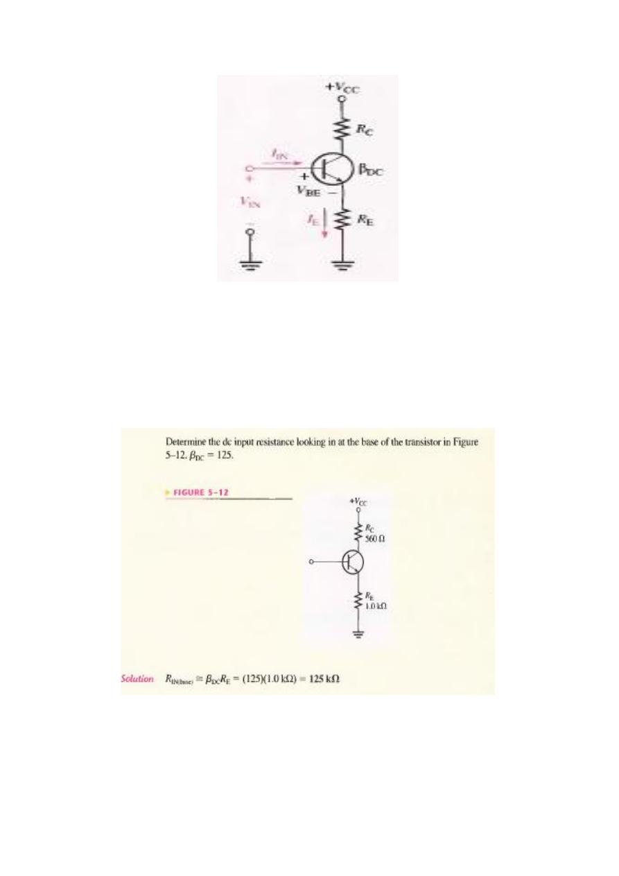
Figure2-8
The input current is the base current:
I
IN
= I
B
By substitution.
Rm(base) = V IN / I
IN
= β
DC
I
B
R
E
/ I
B
RINlbase) = β
DC
R
E
Example
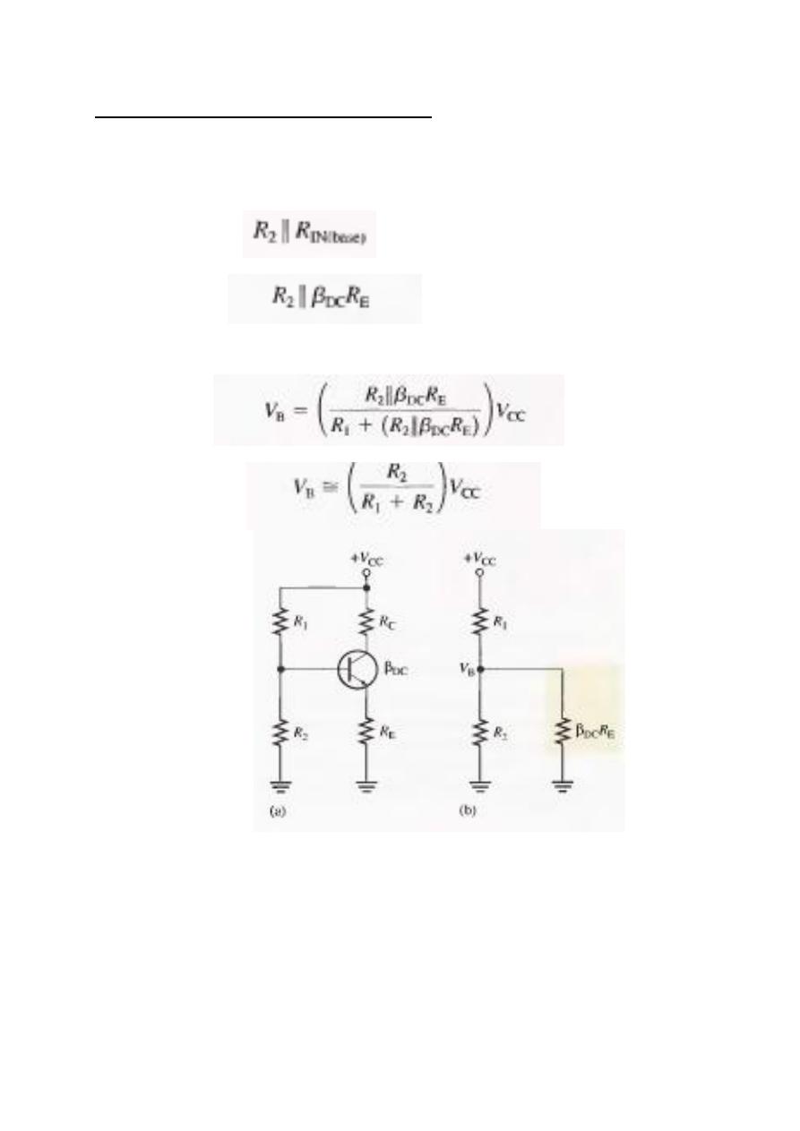
Analysis of a Voltage-Divider Bias Circuit
A voltage-divider biased NPN transistor is shown in Figure 5-13(a). Let's begin the analysis by
determining the voltage at the base using the voltage-divider formula, which is developed as follows:
R
1N
(
base)
=
β
DC
R
E
The total resistance from base to ground is
Substituting R1N(base) = β
DC
R
E
A voltage-divider is formed by R 1 and the resistance from base to ground (β
DC
RE) in para-
llel with Rz as shown in Figure 5-13(b). Applying the voltage-divider formula yields
If βDCRE » Rz (at least ten times greater), then the formula simplifies to
Figure2-9: An npn transistor with voltage- divider bias.
Once you know the base voltage, you can determine the emitter voltage, which equals VB less the
value of the base-emitter drop (V BE ).
V E = VB - V BE
You can find the emitter current by using Ohm's law.
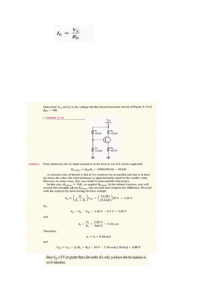
Once you know IE, you can find all the other circuit values
Ic = I
E
V
C
= V cc – IcRc
Once you know V e and V E , you can determine V CE .
V
CE
= Vc - V
E
Also, you can express V CE in terms of Ic by using Kirchhoff's voltage law as follows:
V cc- IcRc - I
E
R
E
- V
CE
= 0
Since Ic = I
E
,
V
CE
== Vcc - IcRc - IcRE
V CE == V cc - Ic(Rc + R
E
)
Example
Stability of Voltage-Divider Bias
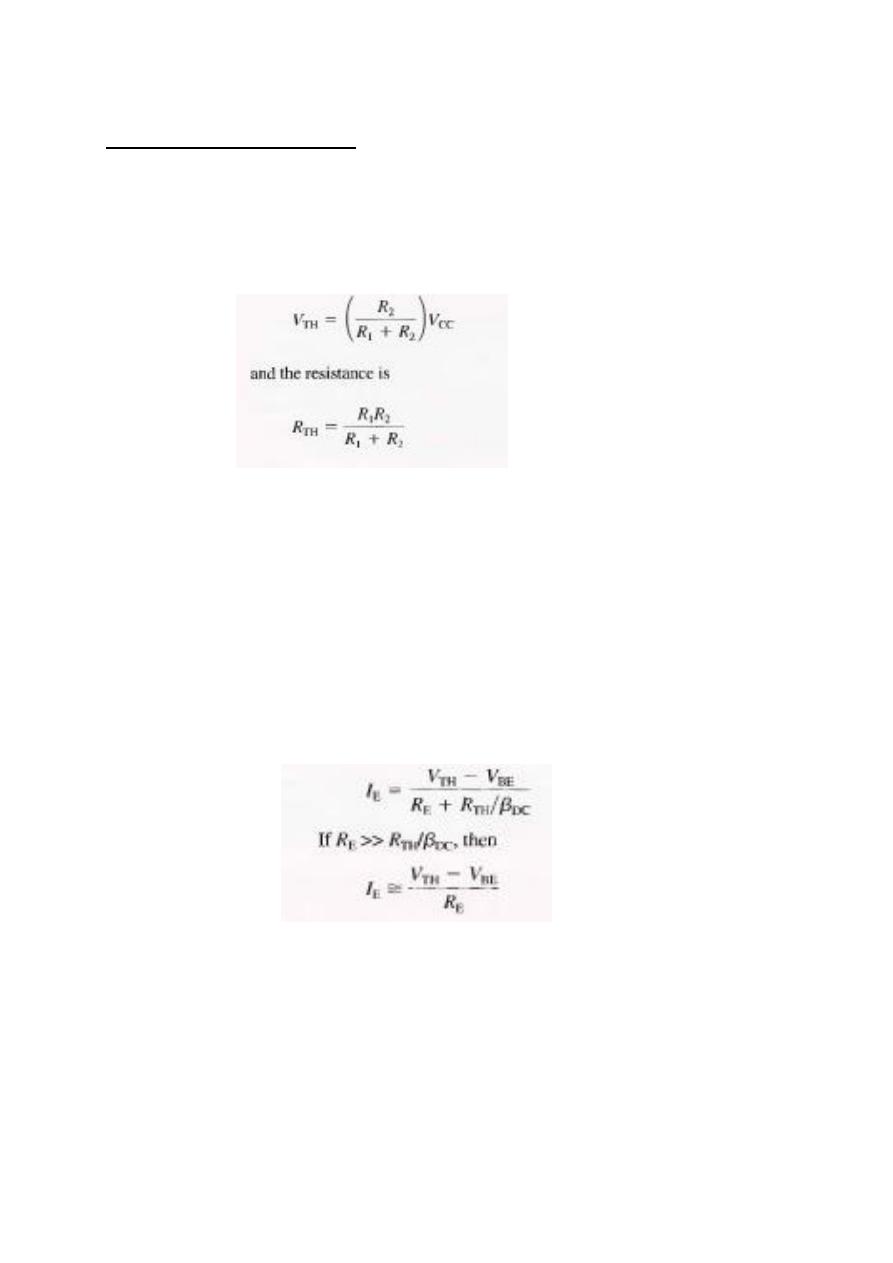
Another way to analyze a voltage-divider biased transistor circuit is to apply Thevenin's the-
orem. We will use this method to evaluate the stability ofthe circuit. First, let's get an equiv-
alent base-emitter circuit for Figure 5-13 using Thevenin's theorem. Looking out from the
base terminal, the bias circuit can be redrawn as shown in Figure 5-15(a). Apply Thevenin's
theorem to the circuit left of point A, with V ee replaced by a short to ground and the tran-
sistor disconnected from the circuit. The voltage at point A with respect to ground is
The Thevenin equivalent of the bias circuit, connected to the transistor base, is shown in the
beige box in Figure 2-10(b). Applying Kirchhoff's voltage law around the equivalent base-
emitter loop gives
V
TH
- V
RTH
- V
BE
- V
RE
= 0
Substituting. using Ohm's law, and solving for V
TH
,
V
TH
= I
B
R
TH
+ V
BE
+ I
E
R
E
Substituting I E / β
DC
for I B ,
V TH = IE(R
E
+ R
TH
/ β
DC
+ V
BE
or, solving for IE,
This last equation shows that IE, and therefore Ic, is independent of {3DC {notice that {3DC
does not appear in the equation) for the stated condition. This can be achieved in practice
by selecting a value for R E that is at least ten times the resistance of the parallel combina-
tion of the voltage-divider resistors (R TH ) divided by the minimum {3DC'
Voltage-divider bias is widely used because reasonably good stability is achieved with a
single supply voltage.
Figure2-10: Thevenizing the bias circuit.
Voltage-Divider Biased PNP Transistor
As you know, a pnp transistor requires bias polarities opposite to the npn. This can be ac-
complished with a negative collector supply voltage. as in Figure 5-16(a), or with a posi-
tive emitter supply voltage, as in Figure 2-11(b). In a schematic, the pnp is often drawn
upside down so that the supply voltage line can be drawn across the top of the schematic
and ground at the bottom, as in Figure 2-12. The analysis procedure is basically the same
as for an npn transistor circuit, as demonstrated in the following steps with reference to
Figure 2-12. The base voltage is determined by using the voltage-divider formula.
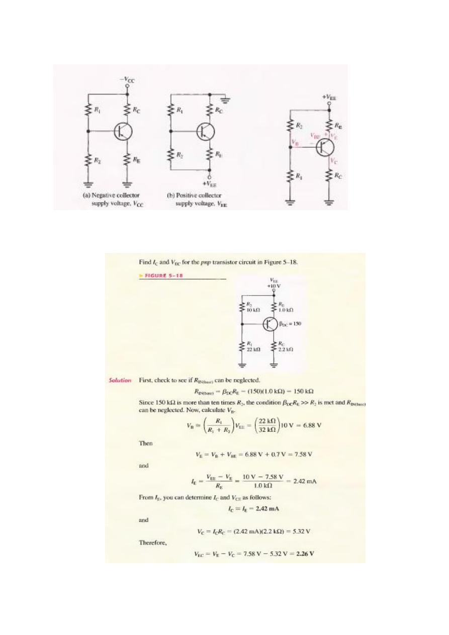
Figure2-11 Figure2-12
Example
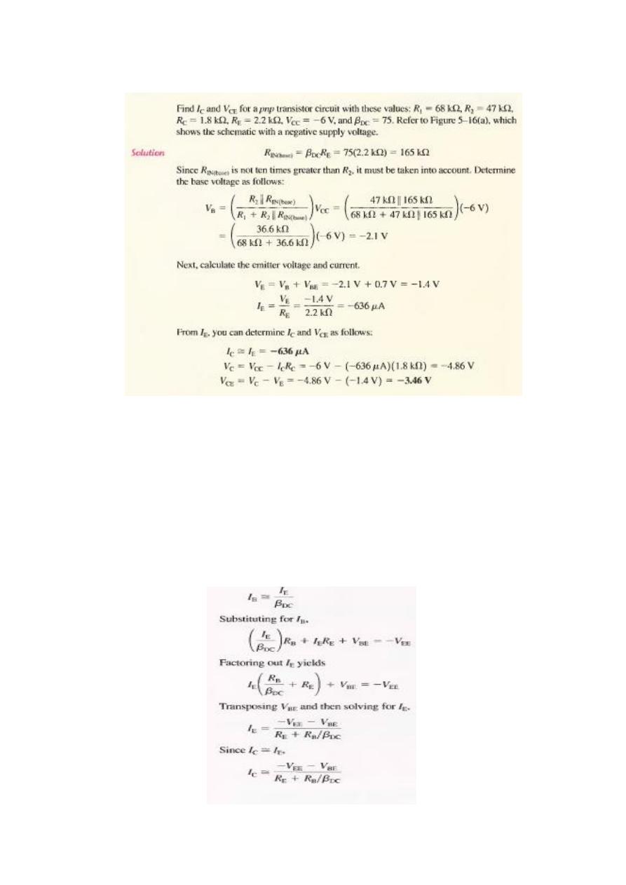
Example
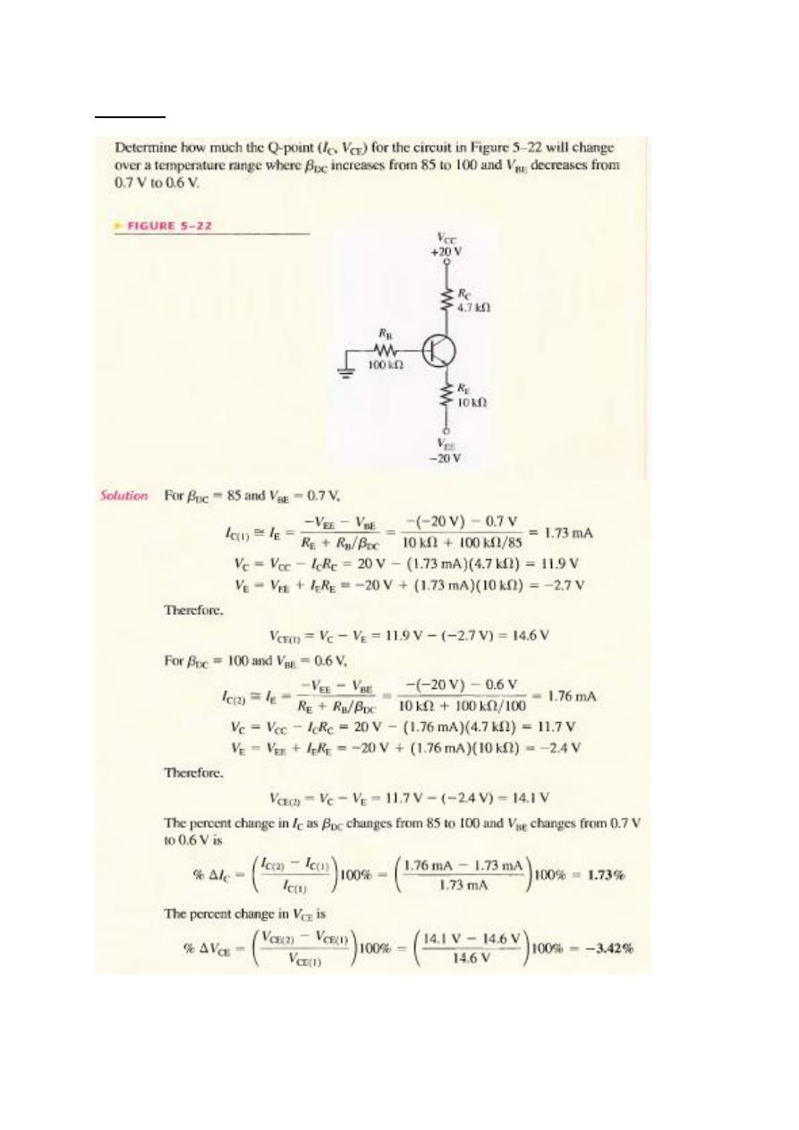
Emitter Bias
Emitter bias uses both a positive and a negative supply voltage. In the circuit shown in
Figure 2-13, the V EE supply voltage forward-biases the base-emitter junction. Kirchhoff's
voltage law applied around the base-emitter circuit in part (a), which has been redrawn in
part (b) for analysis. gives the following equation:
V EE + V RB + V BE + V RE = 0
Substituting, using Ohm's law,
V EE + IBR B + V BE + IER E = 0
Solving for V EE ,
IBR B + IER E + V BE = - V EE
Since Ic = IE and Ic = β
DC
IB'
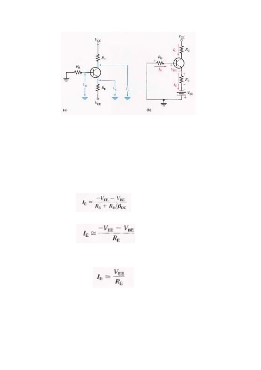
Figure2-13: An npn transistor with emitter bias. Polarities are reversed for a pnp
transistor. Single subscripts indicate voltages with respect to ground.
Voltages with respect to ground are indicated by a single subscript. The emitter voltage with
respect to ground is
V E = V EE + IER L
The base voltage with respect to ground is
VB = V E + V BE
The collector voltage with respect to ground is
V c = V CC - IcRc
Q-Point Stability of Emitter Bias The formula for IE shows that the emitter bias circuit is
dependent on V BE andβ
DC
, both of which change with temperature and current.
If R E » R B /[3oc, the R B /{3oc term can be dropped and the equation becomes
This condition makes IE essentially independent of {3oc.
A further approximation can be made; if V EE » V BE , the V BE term can be dropped.
This condition makes IE essentially independent of V BE .
If IE is independent of βDC and V BE , then the Q-point is not affected by variations in these
parameters. Thus, emitter bias can provide a stable Q-point if properly designed.
Example
Collector-Feedback Bias
In Figure 2-14, the base resistor RB is connected to the collector rather than to V cc , as it
was in the base bias arrangement discussed earlier. The collector voltage provides the bias for
the base-emitter junction. The negative feedback creates an "offsetting" effect that tends to
keep the Q-point stable. If Ic tries to increase, it drops more voltage across Rc, thereby caus-
ing V c to decrease. When V c decreases, there is a decrease in voltage across R B , which
decreases lB. The decrease in I B produces less Ic which, in turn, drops less voltage across Rc
and thus offsets the decrease in V c .
Analysis of a Collector-Feedback Bias Circuit By Ohm's law, the base current can be
expressed as
Let's assume that Ic» lB' The collector voltage is
V c == V cc – IcRc
Also,
Substituting for I B and V e in the equation I B = (Ve - VBE)/R B ,
The terms can be arranged so that
Then you can solve for le as follows:
Since the emitter is ground, V
CE
= V
C
.
V
CE
= V
CC
– l
C
R
C
Fxample
SELF TEST:
1. The maximum value of collector current in a biased transistor is
(a) f3DcIB (b) IC(satl (e) greater than IE (d) IE - IB
2. Ideally, a de load line is a straight line drawn on the collector characteristic
curves between
(a) the Q-point and cutoff (b) the Q-point and saturation
(e) VCE(cutoft) and ICCsatl (d) IB = 0 and IB = Ic/f3Dc
3. If a sinusoidal voltage is applied to the base of a biased npn transistor and the
resulting
sinusoidal collector voltage is clipped near zero volts. the transistor is
(a) being driven into saturation (b) being driven into cutoff
(e) operating nonlinearly (d) answers (a) and (c) (e) answers (b) and (c)
4. The input resistance at the base of a biased transistor depends mainly on
(a) f3DC (b) R B (e) R E (d) f3DC and R E
5. In a voltage-divider biased transistor circuit such as in Figure 5-13, RINtbasel
can generally be
neglected in calculations when
(a) R!N(baseJ > Rz (b) Rz> IOR!NCbasel (el R.N(baseJ> lORz (d) Rl «Rz
6. In a certain voltage-divider biased npn transistor, VB is 2.95 V. The dc
emitter voltage is
approximately

(a) 2.25 V
(b) 2.95 V
(e) 3.65 V
(d) 0.7 V
7. Voltage-divider bias
(a) cannot be independent of β
DC
(b) can be essentially independent of β
DC
(e) is not widely used
(d) requires fewer components than all the other methods
8. The disadvantage of base bias is that
(a) it is very complex (b) it produces low gain
(e) it is too beta dependent (d) it produces high leakage current
9. Emitter bias is
(a) essentially independent of f3DC (b) very dependent on f30c
(e) provides a stable bias point (d) answers (a) and (c)
10. In an emitter bias circuit, R E = 2.7 kQ and V EE = 15 V. The emitter
current
(a) is 5.3 mA (b) is 2.7 mA (e) is 180 mA (d) cannot be detennined
11. Collector-feedback bias is
(a) based on the principle of positive feedback
(e) based on the principle of negative feedback
(b) based on beta multiplication
(d) not very stable
12. In a voltage-divider biased npn transistor. if the upper voltage-divider
resistor (the one
connected to V cc ) opens,
(a) the transistor goes into cutoff (b) the transistor goes into saturation
(c) the transistor burns out (d) the supply voltage is too high
13. In a voltage-divider biased npn transistor. if the lower voltage-divider
resistor (the one
connected to ground) opens,
(a) the transistor is not affected (b) the transistor may be driven into cutoff
(c) the transistor may be driven into saturation (d) the collector current will
decrease
14. In a voltage-divider biased pnp transistor, there is no base current. but the
base voltage is
approximately correct. The most likely problem(s) is
(a) a bias resistor is open (b) the collector resistor is open
(c) the base-emitter junction is open (d) the emitter resistor is open
(e) answers (a) and (c) (I) answers (c) and (d)
Problems:
1. The output (collector voltage) of a biased transistor amplifier is shown in
Figure 2-13. Is the transistor biased too close to cutoff or too close to
saturation?
Fig.2-13
2. Determine the intercept points of the dc load line on the vertical and
horizontal axes of the collector-characteristic curves for the circuit in Figure 2-
14.
Fig. 2-14
3. Assume that you wish to bias the transistor in Figure 2-14 with I B = 20 μt.to
what voltage must you change the V
BB
supply? What are Ic and V
CE
at the Q-
point, given that β
DC
= 50?
4. Design a biased-transistor circuit using V BB = V cc = 10 V for a Q-point of
Ic = 5 mA and V CE = 4 V. Assume β
DC
= 100. The design involves finding
RB, Rc and the minimum power rating of the transistor. (The actual power
rating should be greater.) Sketch the circuit.
5 Determine whether the transistor in Figure 2-15 is biased in cutoff, saturation,
or the linear region. Keep in mind that Ic = βI
B
is valid only in the linear region.
Fig.2-15
6. What is the minimum value of βDC in Figure 2-15 that makes
RIN(base) = 10 R2 ?
7. The bias resistor R2 in Figure 2-15 is replaced by a 15 kΩ potentiometer.
What minimum resistance setting causes saturation?
8. If the potentiometer described in Problem 10 is set at 2 kΩ, what are the
values for IC and V CE ?
9. Determine all transistor terminal voltages with respect to ground in
Fig.2-16. Do not neglect the input resistance at the base or V BE .
10. Show the connections required to replace the transistor in Figure 2-16 with a
PNP device.
Fig.2-15
Dig.2-16
11. Determine IB, Ic, and VCE for a base-biased transistor circuit with the
following values: βDC = 90. V cc = 12 V. R B = 22 kΩ and Rc = 100 Ω.
12. If βDC in Problem 11 doubles over temperature, what are the Q-point
values?
13. You have two base bias circuits connected for testing. They are identical
except that one is biased with a separate V BB source and the other is biased
with the base resistor connected to V cc . Ammeters are connected to measure
collector current in each circuit. You vary the V cc
supply voltage and observe that the collector current varies in one circuit. but
not in the other.
In which circuit does the collector current change? Explain your observation.
The data sheet for a particular transistor specifies a minimum f30c of 50 and a
maximum f30c
of 125. What range of Q-point values can be expected if an attempt is made to
mass-produce
the circuit in Figure 5--42? Is this range acceptable if the Q-point must remain
in the
transistor's linear region?

CHAPTER THREE
