The purpose of this experiment is to introduce diode rectifier circuits used in DC
power supplies.
Almost all electronic systems require at least one DC power supply that converts AC line
voltage (most often 120VAC @ 60 Hz) to DC voltage (typically 5 to 20 VDC). To accomplish
this, diodes are used to produce either positive or negative DC voltage from an alternating
source in a process called rectification. The diode is, therefore, an essential element of every
DC power supply.
The purity of DC voltage delivered by the power supply is largely determined by the
requirements of its load (i.e., electronic system). Rectified AC naturally pulsates, and is usually
smoothed by filtering to produce a steady DC value. Perfect filtering would produce a DC
output having no AC variation at all. In practice, some unwanted AC voltage, called “ripple”,
appears at the output along with the desired DC voltage. The ratio of AC ripple voltage to DC
voltage at the power supply output is called “ripple factor”. Ripple factor is defined as either
RMS
DC
V
V
, or
p p
DC
V
V
−
. The peak-to-peak definition is used here, primarily for ease of measurement.
Maximum allowable AC ripple factor and minimum DC current output are usually specified as
part of a power supply’s design requirements.
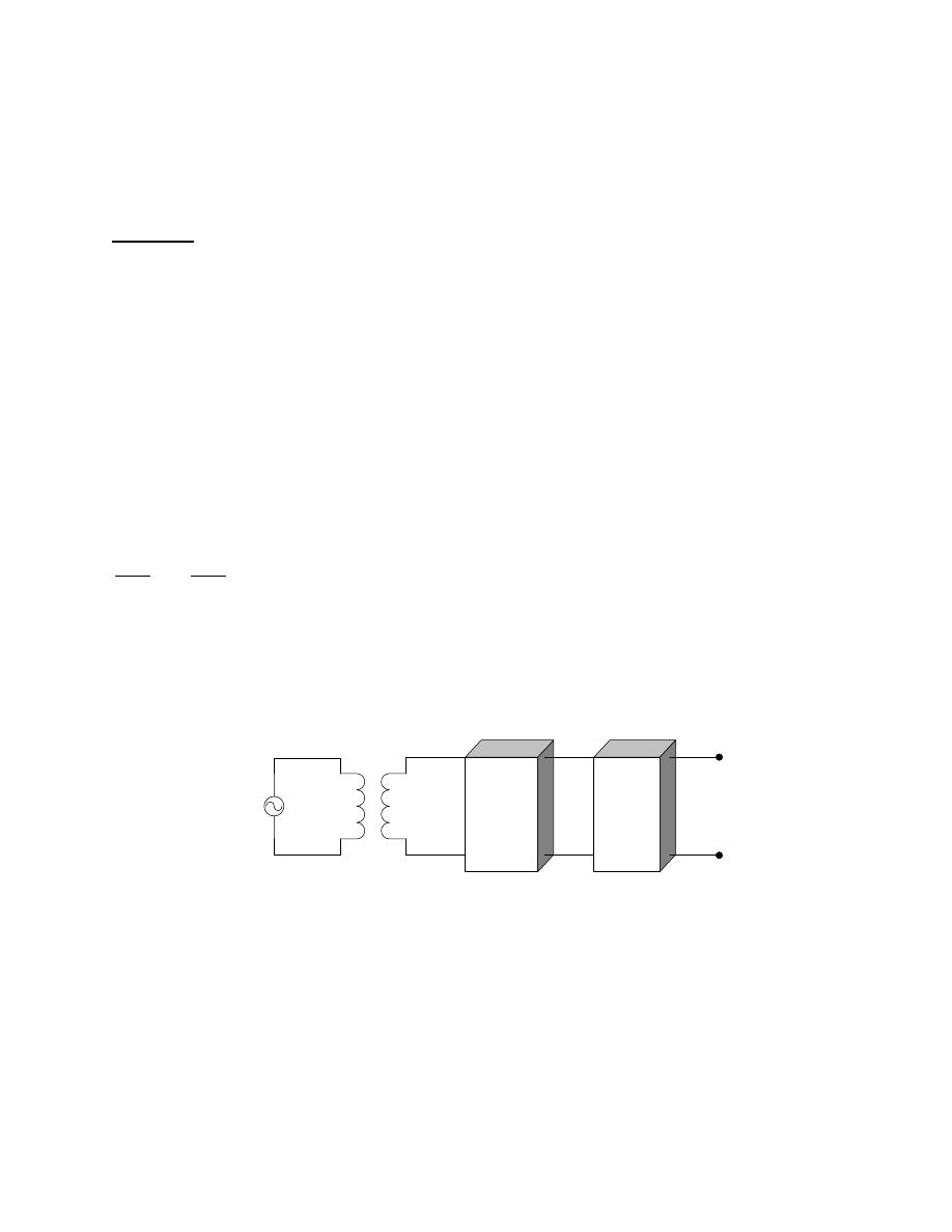
A DC power supply block diagram is shown in Fig. 1.
Diode
Rectifier
Power
Transformer
Filter
120 VAC
+
DC
Output
-
Fig. 1. DC Power Supply Block Diagram
The AC input voltage is stepped down from 120 V to the appropriate level at the rectifier input
by the power transformer. The rectifier converts the sinusoidal voltage to a pulsating, DC
voltage, which is then filtered to produce a relatively low ripple DC voltage at the output. The
type of filter selected depends on load current, ripple specifications, cost, size and other design
requirements. To further reduce the ripple and stabilize the magnitude of the DC output voltage
against variations caused by changing load, a voltage regulator is often employed as well.
Department of Electrical Engineering
Experiment name - Diodes and Bridge Rectifiers
Overview:
When designing a power supply, two important parameters must be specified to assure that
diodes are selected properly: 1) the maximum current capability, which is determined by the
largest current that the diode is expected to conduct, and 2) the peak inverse voltage (PIV),
which is determined by the largest reverse voltage that is expected to appear across it.
Rectifier circuits used in DC power supplies are classified as either half-wave or full-wave types.
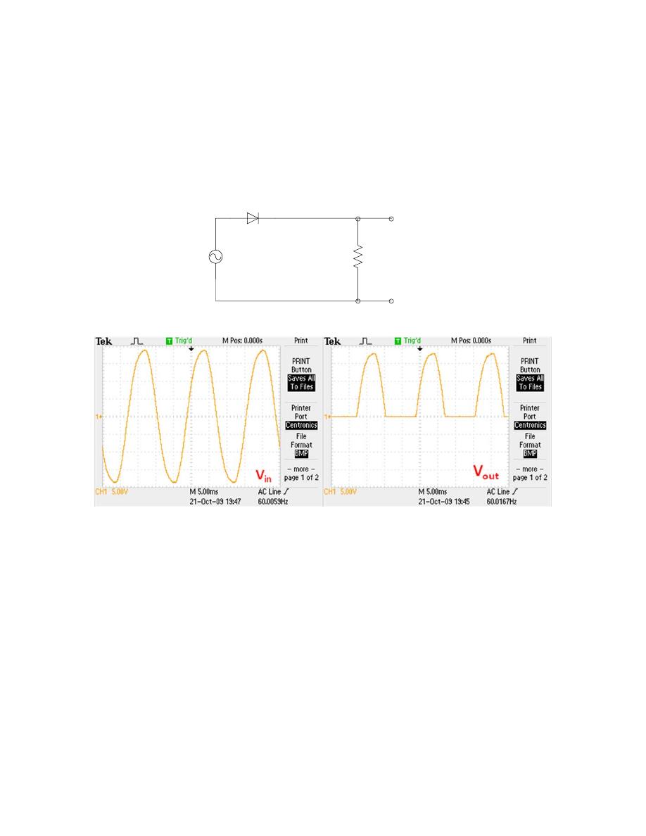
The half-wave rectifier shown in Fig. 2 passes only the positive half-cycles of the sinusoid to the
output, because the diode blocks current flow during the negative half cycles.
V
in
R
L
D
+
V
out
-
Fig. 2. Half Wave Rectifier and Voltage Waveforms
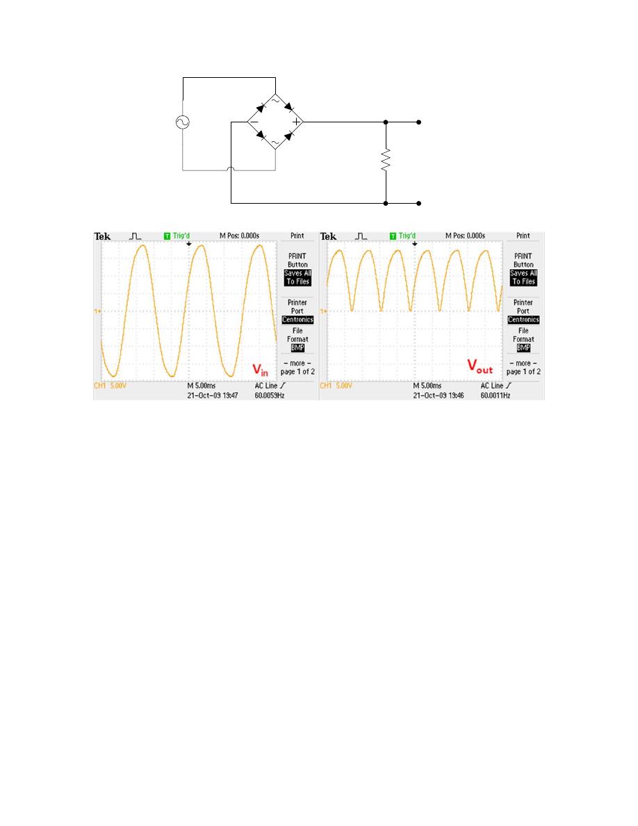
The full-wave bridge rectifier circuit shown in Fig. 3 inverts the negative half-cycles of the
sinusoidal input voltage and passes both half-cycles of each alternation to the output.
During the positive half-cycles of the input voltage, current in the full-wave bridge rectifier is
conducted from the positive terminal of the source, through D1, through the load (resistor)
connected to the output, and then through D2 to return to the source. During the negative half-
cycles of the input voltage, current is conducted from the negative terminal of the source,
through D3, through the load, and then through D4 and back to the source. Note that the load
current’s direction is the same for both positive and negative half-cycles.
V
in
R
L
+
V
out
-
D
1
D1
D
2
D
4
D
3
Figure 3. Full-Wave Bridge Rectifier and Voltage Waveforms
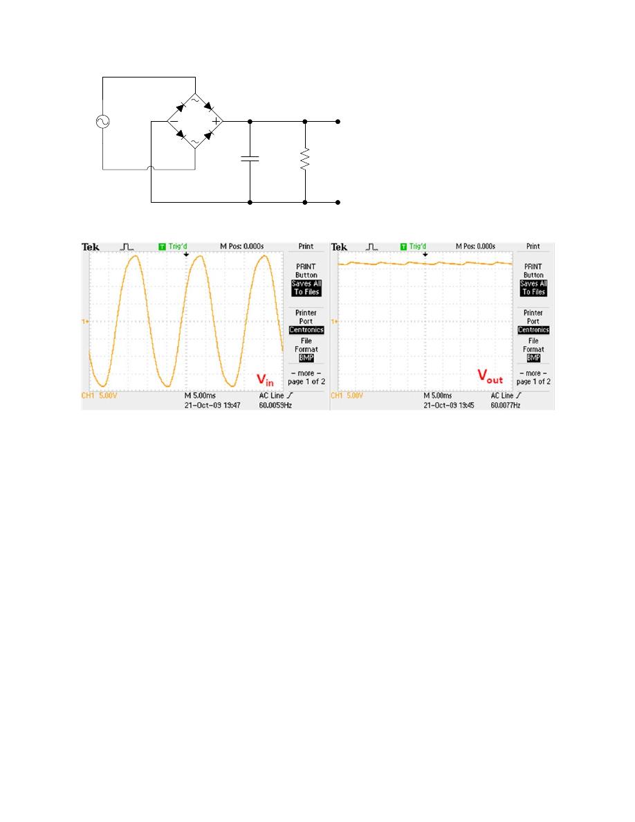
If a simple capacitor filter is connected to the rectifier output as in Fig. 4, the output voltage is
smoothed and approaches its ideal DC value. The capacitor charges up while the diodes are
conducting, and then discharges when the diodes are not conducting to maintain current flow
through the load. When load current is small, ripple are low and the diodes conduct high current
for a very short part of the cycle, transferring charge from the source to the capacitor by means
of large current spikes.
V
in
C
R
L
+
V
out
-
D
1
D1
D
2
D
4
D
3
Figure 4. Filtered Full-Wave Bridge Rectifier and Voltage Waveforms
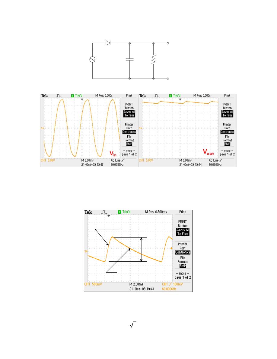
A capacitor filter at the output of a half-wave rectifier (Fig.5) also results in smoothing of the
output, but it is less effective than in the full-wave bridge because the voltage peaks are twice
as far apart in time, necessitating a deeper discharge of the filter capacitor between intervals of
diode conduction.
V
in
C
R
L
D
+
V
out
-
Fig. 5. Filtered Half-Wave Rectifier and Voltage Waveforms
Fig. 6 is an expanded view of the output voltage ripple of Fig. 5, captured using AC oscilloscope
coupling.
V
out
V
p-p
diode on (charging)
diode off
(discharging)
Fig. 6. Filtered Half-Wave Rectifier Ripple Voltage
Peak voltage at the output is given by
2
p
inRMS
D
V
V
V
=
−
, where
D
V
is the forward voltage drop

across the conducting diode. The filter capacitor discharges with time constant
L
R C
between
voltage peaks, which occur with period
T
. Peak-to-peak ripple voltage (
r
V
) for the filtered half-
wave rectifier may, therefore, be approximated by
2
p
inRMS
D
r
p p
L
r
L
V
V
V
V
V
T
R C
f R C
−
−
=
=
=
, where
r
f
is the ripple frequency.

lab calculations for:
a) Ripple frequency, f
r
b) Peak output voltage V
p
c) Peak-to-peak ripple voltage, V
p-p
d) Load (resistor) current, I
L
e) Diode average current, I
D(av)
f) Diode maximum current, I
D(max)
Perform these calculations for both the full-wave bridge rectifier, and the half-wave rectifier
(blown diode) configuration.
Present and compare the calculated results alongside measured results in a table of values.
Comment on the differences between calculated and measured results.
2) Use three different methods to determine load currents for both cases:
•
(
)
(
)
out average
L average
L
V
I
R
=
•
out
L
V
I
C
T
∆
=
∆
during capacitor discharge
•
1
L
s
V
I
R
=
at the mid-point of the capacitor discharge period
Using measured values, apply the above methods to determine load current, I
L
, and
comment on the differing results. Explain why the “slope” method is the least accurate.
3) Using your recorded waveforms and scaling factors for the full-wave bridge rectifier circuit,
first determine the load current waveform
( )
L
i t
and capacitor current waveform
( )
c
i t
, and
then apply Kirchoff’s Current Law to find the diode
current waveform
( )
D
i t
. Include the three
current waveforms in your report and comment on their relationships to each other.
Report – Diodes and Bridge Rectifiers
1) Using the measured values for V
in
,R
L
, R
S
, C and diode forward voltage drop, repeat the pre-