Object:
To examine the Common collector (CC) Amplifier characteristic of transistor.
Apparatus:
1. Two DC power supply.
2. Function generator.
3. AVOmeter.
4. Oscilloscope.
5. Transistor, Resistors 1 KΩ and 100 KΩ, Capacitors 1µf.
THEORY
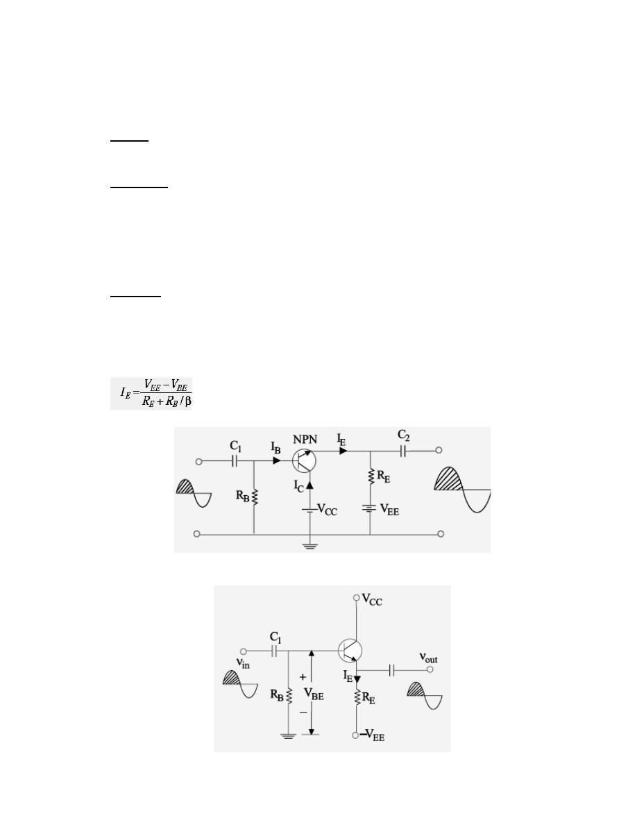
Fig.1 and 2 show the circuit of a single-stage CC amplifier using an NPN transistor. The input
signal is injected into the base-collector circuit and output signal is taken out from the emitter-
collector circuit. The E/B junction is forward-biased by V
EE
and C/B junction is reverse-biased
by V
CC
. The quiescent values of I
B
and I
E
are set by V
CC
and V
EE
together with R
B
and R
E
. As
seen from Fig. 2.
Fig. 1
Fig. 2
Electrical Engineering Ddepartment
2nd class lab.
Common collector Amplifier
Circuit Operation
When positive half-cycle of the signal is applied, then
1. forward bias is increased since V
BE
is positive w.r.t. collector i.e. ground,
2. base current is increased,
3. emitter current is increased,
4. drop across R
E
is increased,
5. hence, output voltage (i.e. drop across R
E
is increased).
Consequently, we get positive half-cycle of the output. It means that a positive-going input
signal results in a positive going output signal and, consequently, the input and output signals
are in phase with each other as shown in Fig. 2.
Characteristics of a CC Amplifier
A CC amplifier has the following characteristics :
1. high input impedance (20-500 K),
2. low output impedance (50-1000 Ω),
3. high current gain of (1 + β) i.e. 50 – 500,
4. voltage gain of less than 1,
5. power gain of 10 to 20 dB,
6. no phase reversal of the input signal.
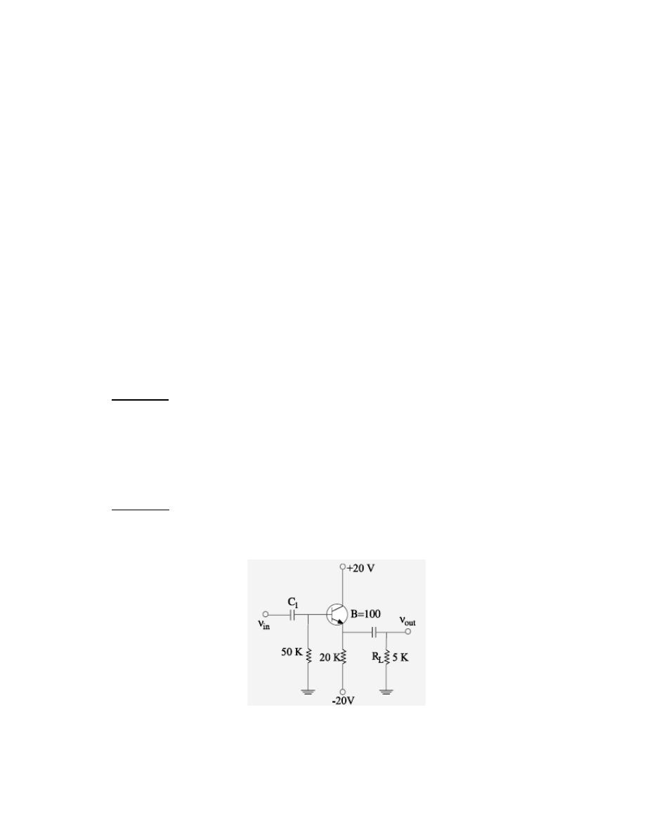
Procedure:
Consider the circuit shown in Fig. (3), it is a single stage amplifier
1- Connect the circuit.
2- Give an input to the amplifier so that the output is 4Vpp at 1 kHz Measure the input
voltage (f=1 kHz).
3- Give an input of 0.5V p-p to the amplifier.
Discussion:
1. Determine Ai, Av, and Ap.
2. What is the effect of Rb on amplifier?
Fig. 3