
ISSUES TO ADDRESS...
•
What types of defects arise in solids?
• Can the number and type of defects be varied
and controlled?
• How do defects affect material properties?
• Are defects undesirable?
• How do point defects in ceramics differ from those
in metals?
• In ceramics, how are impurities accommodated
in the lattice and how do they affect properties?
1
CHAPTER 5:
IMPERFECTIONS IN SOLIDS

The properties of some materials are profoundly influenced
by the presence of imperfections. Consequently,
it is important to have a knowledge about the types of
imperfections that exist and the roles they play in affecting
the behavior of materials. For example, the mechanical
properties of pure metals experience significant
alterations when alloyed (i.e., when impurity atoms are
added)—for example, brass (70% copper–30% zinc) is
much harder and stronger than pure copper (Section
7.9).
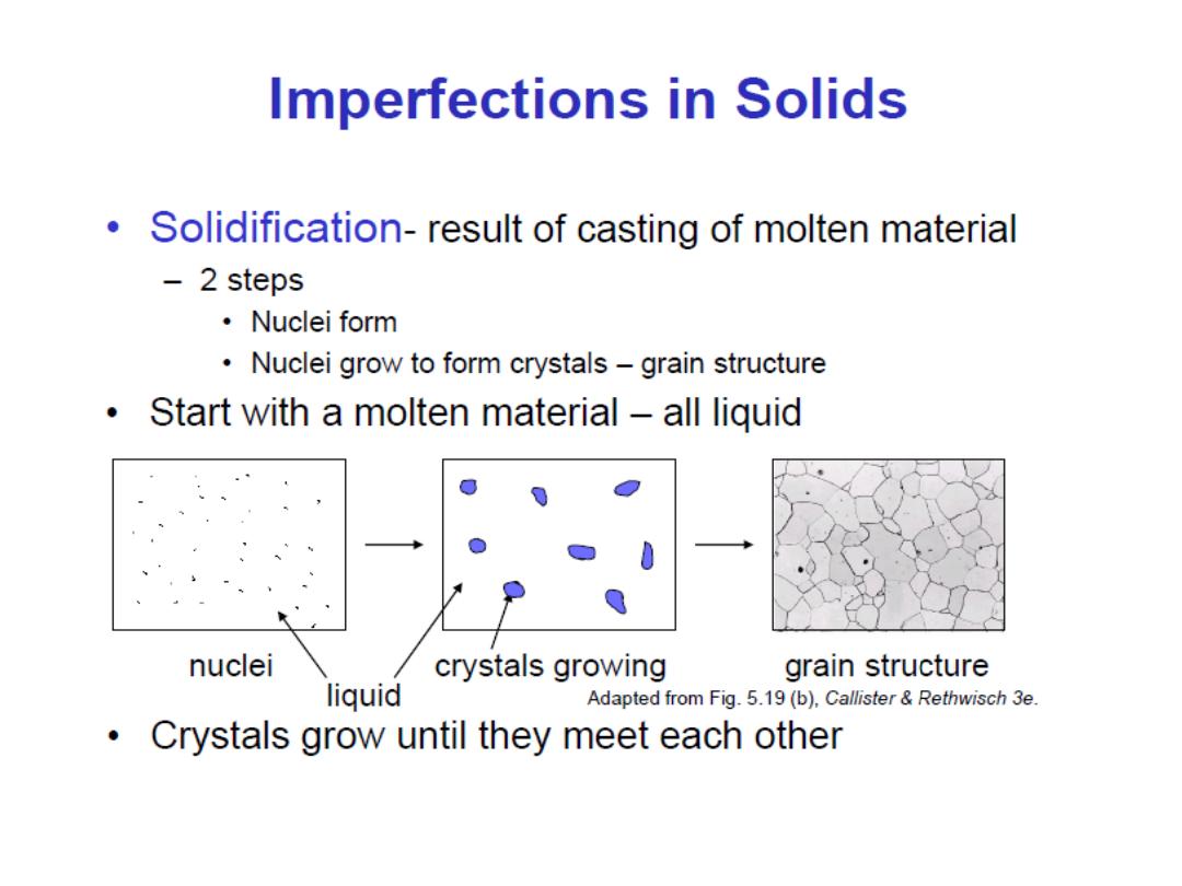
Why study Imperfections in solids?

Thus far it has been tacitly assumed that perfect order exists
throughout crystalline materials on an atomic scale. However, such
an idealized solid does not exist; all contain large numbers of
various defects or imperfections.

2
TYPES OF IMPERFECTIONS
By “crystalline defect” is meant a lattice irregularity having one or
more of its dimensions on the order of an atomic diameter.
Classification of crystalline imperfections is frequently made according
to geometry or dimensionality of the defect.
Several different imperfections are discussed in this chapter, including
point defects (those associated with one or two atomic positions), linear
(or one-dimensional) defects, as well as interfacial defects, or
boundaries, which are two-dimensional.

2
• Vacancy atoms
• Interstitial atoms
• Substitutional atoms
• Dislocations
• Grain Boundaries
Point defects
Line defects
Area defects
TYPES OF IMPERFECTIONS

The simplest of the point defects is a
vacancy
, or vacant lattice site,one
normally occupied from which an atom is missing.
A
self-interstitial
is an atom from the crystal that is crowded into an
interstitial site, a small void space that under ordinary circumstances
is not occupied.

Impurity point defects
are found in solid solutions, of which
there are two types: substitutional and interstitial. For the
substitutional type, solute or impurity atoms replace or
substitute for the host atoms.
There are several features of the solute and solvent atoms that
determine the degree to which the former dissolves in the latter.
1. Atomic size factor
2. Crystal structure
3. Electronegativity
4. Valences
3
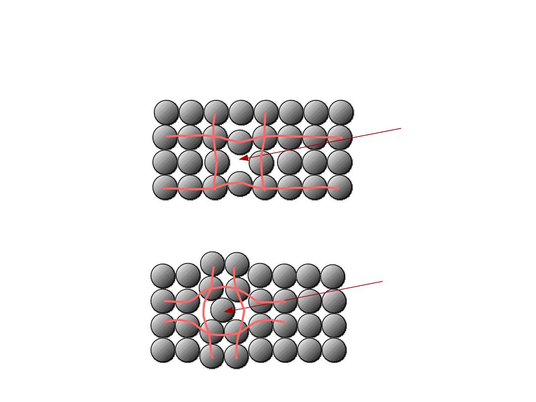
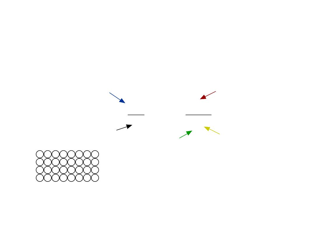
•
Vacancies
:
-vacant atomic sites in a structure.
Vacancy
distortion
of planes
•
Self-Interstitials
:
-"extra" atoms positioned between atomic sites.
self-
interstitial
distortion
of planes
POINT DEFECTS
Boltzmann's constant
(1.38 x 10⁻²³ J/atom K)
(8.62 x 10⁻⁵ eV/atom K)
N
D
N
exp
Q
D
k
T
No. of defects
No. of potential
defect sites.
Activation energy
Temperature
Each lattice site
is a potential
vacancy site
4
• Equilibrium concentration varies with temperature!
EQUIL. CONCENTRATION:
POINT DEFECTS
5
• We can get Q from
an experiment.
• Measure this...
• Replot it...
1/
T
N
ND
ln
1
-
QD
/k
slope
MEASURING ACTIVATION
ENERGY
6
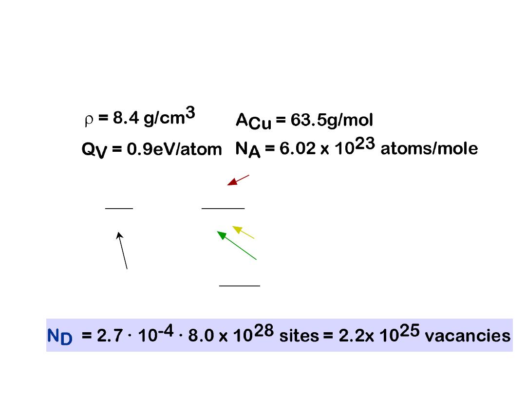
• Find the equil. # of vacancies in 1m of Cu at 1000C.
• Given:
3
8.62 x 10⁻⁵ eV/atom-K
0.9eV/atom
1273K
N
D
N
exp
Q
D
k
T
For 1m3, N =
NA
ACu
x
x 1m3 = 8.0 x 1028 sites
= 2.7
· 10
-4
• Answer:
ESTIMATING VACANCY CONC.
7
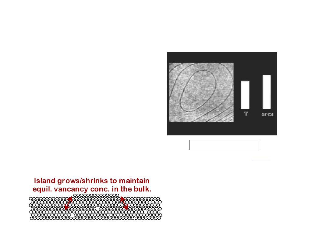
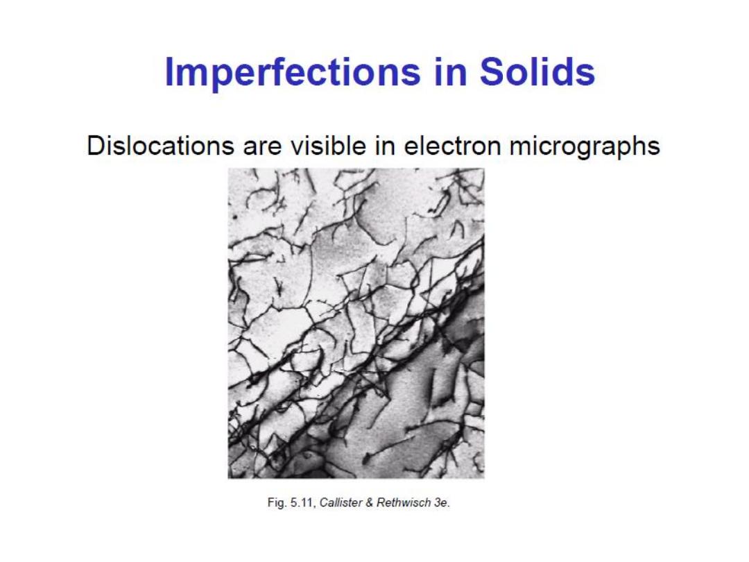
• Low energy electron
microscope view of
a (110) surface of NiAl.
• Increasing T causes
surface island of
atoms to grow.
• Why?
The equil. vacancy
conc. increases via atom
motion from the crystal
to the surface, where
they join the island.
Reprinted with permission from
(K.F.
McCarty, J.A. Nobel, and N.C. Bartelt, "Vacancies in
Solids and the Stability of Surface Morphology",
Nature, Vol. 412, pp. 622-625 (2001). Image is
5.75
mm by 5.75 mm.) Copyright (2001) Macmillan
Publishers, Ltd.
OBSERVING EQUIL. VACANCY CONC.
Click on image to animate
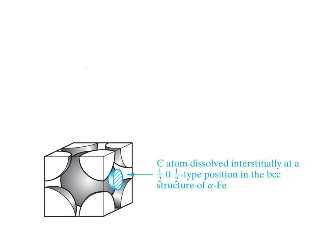
Interstitial solid solution applies to carbon in α-
iron. The carbon atom is small enough to fit with
some strain in the interstice (or opening) among
adjacent Fe atoms in this important steel
structure.
But the interstitial solubility is quite low since the size mismatch of the site to the radius of a
carbon atom is only about 1/4
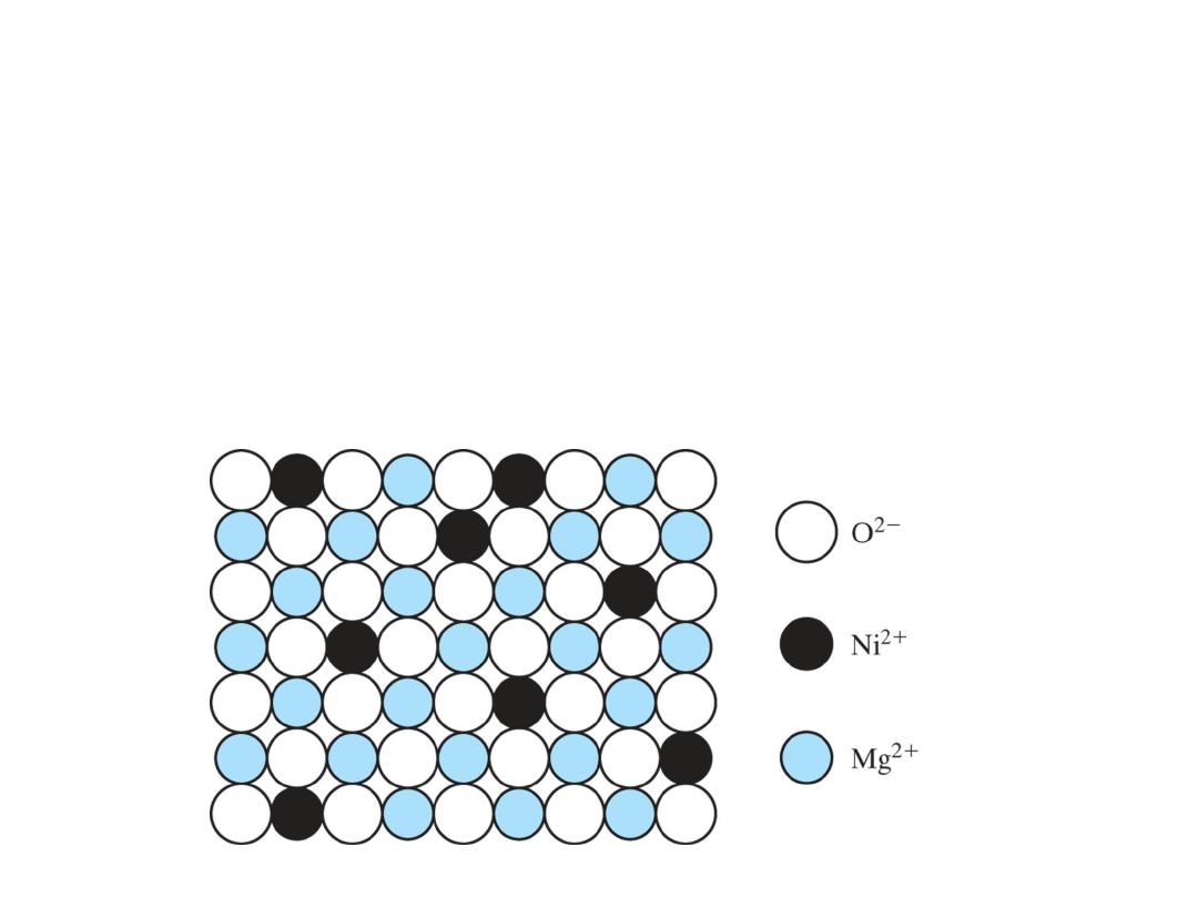
Random, substitution solid solution
can occur in Ionic Crystalline
materials as well. Here of NiO in
MgO. The O
2−
arrangement is
unaffected. The substitution occurs
among Ni
2+
and Mg
2+
ions.
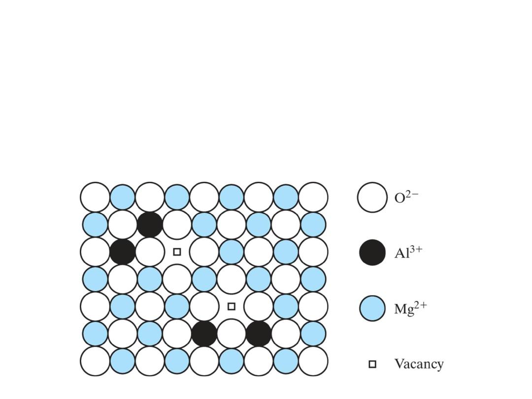
A substitution solid solution of Al
2
O
3
in MgO is
not as simple as the case of NiO in MgO. The
requirement of charge neutrality in the overall
compound permits only two Al
3+
ions to fill
every threeMg
2+
vacant sites, leaving oneMg
2+
vacancy.
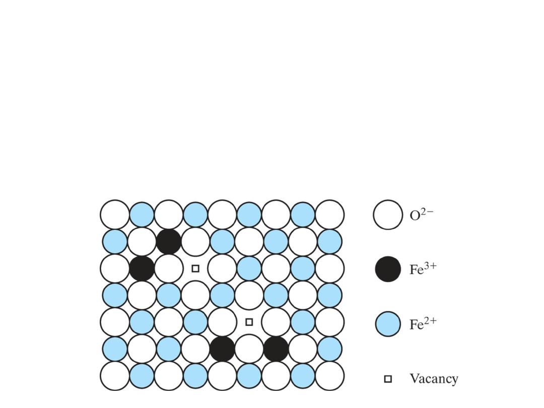
Iron oxide, Fe
1−
x
O with x
≈ 0
.
05
, is an example
of a nonstoichiometric compound. Similar to
the case of Figure 4.6, both Fe
2+
and Fe
3+
ions
occupy the cation sites, with one Fe
2+
vacancy
occurring for every two Fe
3+
ions present.
8
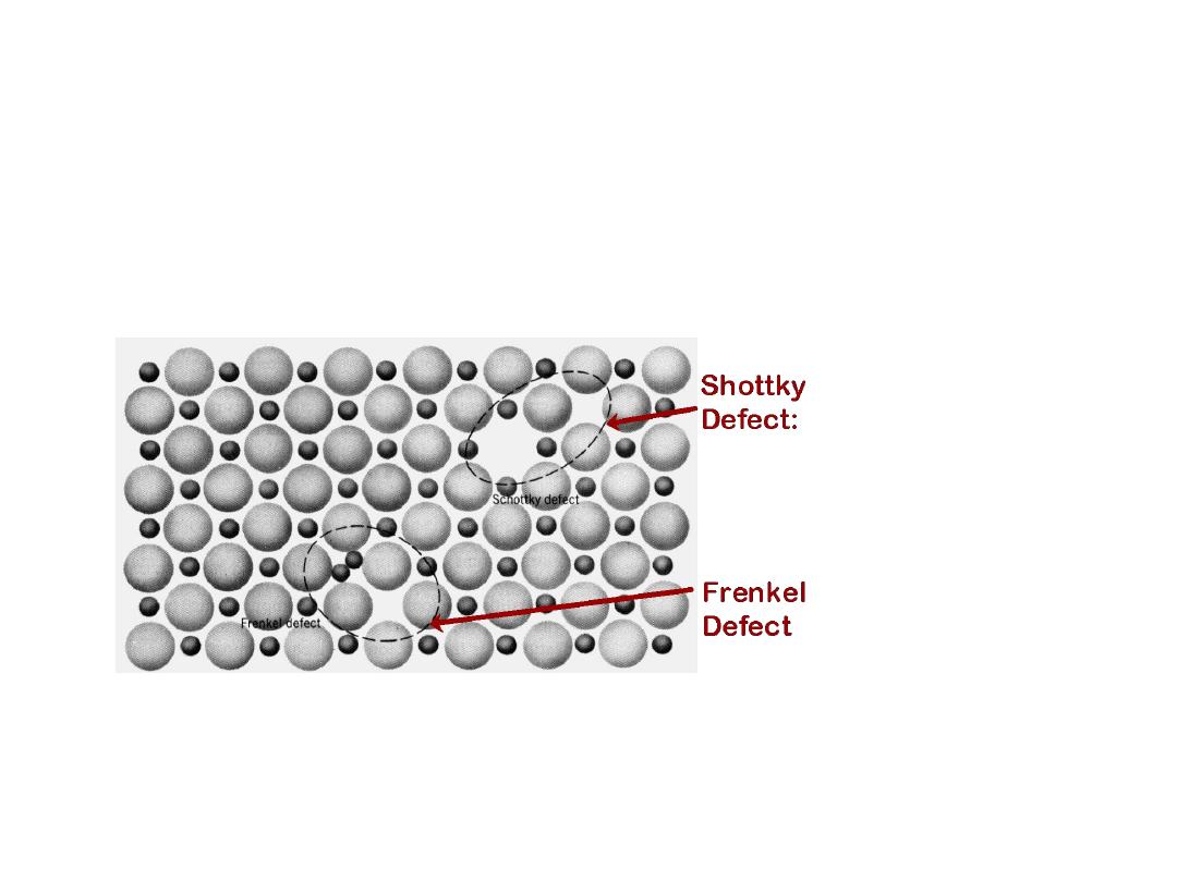
•
Frenkel Defect
--
a cation is out of place.
•
Shottky Defect
--
a paired set of cation and anion vacancies.
•
Equilibrium concentration of defects
~ e
Q
D
/ kT
Adapted from Fig. 13.20,
Callister 5e. (Fig. 13.20 is from
W.G. Moffatt, G.W. Pearsall,
and J. Wulff,
The Structure and
Properties of Materials, Vol. 1,
Structure, John Wiley and
Sons, Inc., p. 78.) See Fig.
12.21,
Callister 6e.
DEFECTS IN CERAMIC
STRUCTURES
9
Two outcomes if impurity (B) added to host (A):
•
Solid solution
of
B
in
A
(i.e., random dist. of point defects)
• Solid solution of
B
in
A
plus particles of a new
phase (usually for a larger amount of B)
OR
Substitutional
alloy
(e.g.,
Cu
in
Ni
)
Interstitial
alloy
(e.g.,
C
in
Fe
)
Second phase particle
--different
composition
--often different structure.
POINT DEFECTS IN ALLOYS
10
• Low energy electron
microscope view of
a (111) surface of Cu.
• Sn islands move along
the surface and "alloy"
the Cu with Sn atoms,
to make "bronze".
• The islands continually
move into "unalloyed"
regions and leave tiny
bronze particles in
their wake.
• Eventually, the islands
disappear.
Reprinted with permission from: A.K. Schmid,
N.C. Bartelt, and R.Q. Hwang, "Alloying at
Surfaces by the Migration of Reactive Two-
Dimensional Islands", Science, Vol. 290, No.
5496, pp. 1561-64 (2000). Field of view is 1.5
mm and the temperature is 290K.
ALLOYING A SURFACE
Click on image to animate
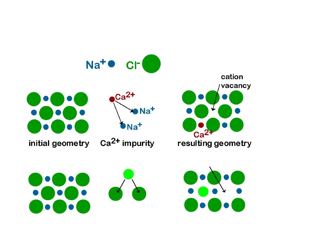
11
•
Impurities must also satisfy
charge balance
•
Ex: NaCl
•
Substitutional cation impurity
•
Substitutional anion impurity
initial geometry
O2- impurity
O2-
Cl-
anion vacancy
Cl-
resulting geometry
IMPURITIES

12
It is often necessary to express the
composition
(or
concentration) of an alloy in terms of its constituent
elements.
The two most common ways to specify composition
are
weight
(or mass) percent and
atom
percent.
COMPOSITION
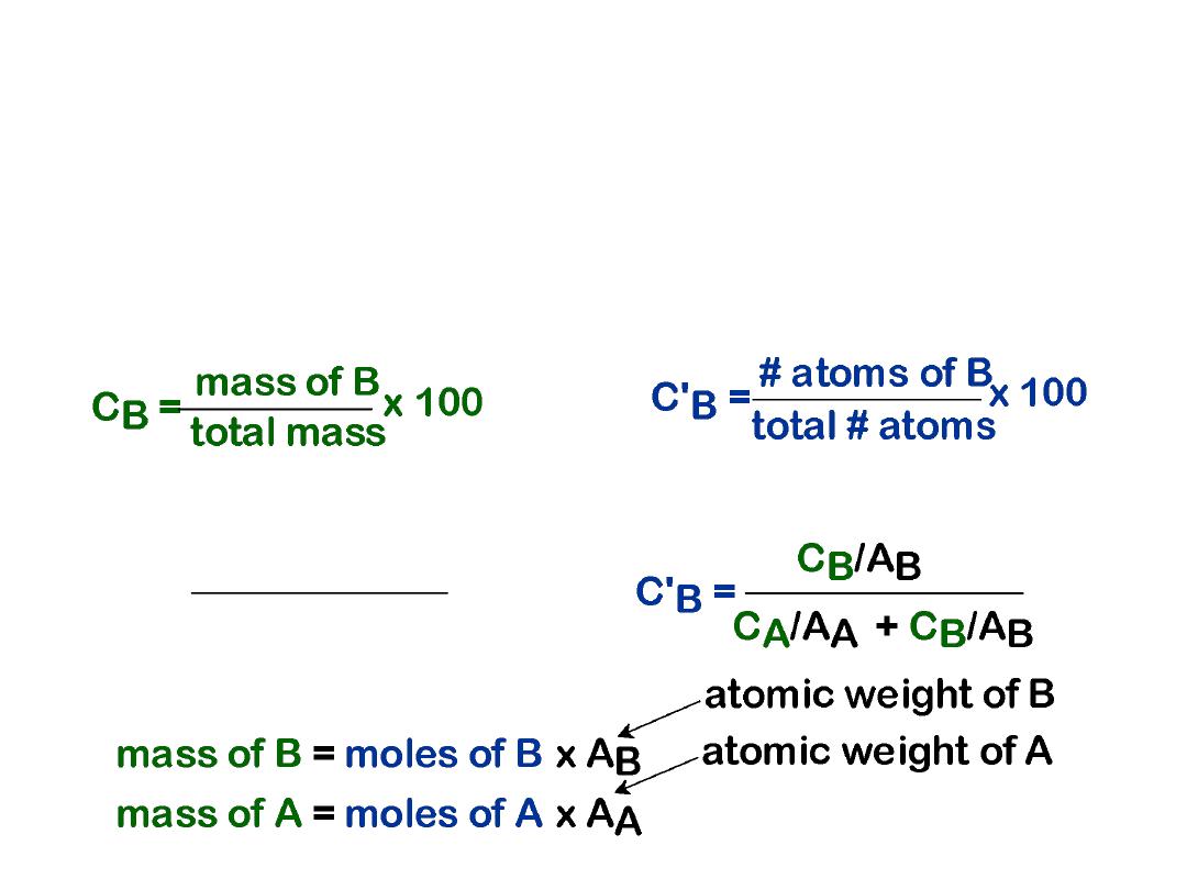
12
• Weight %
Two descriptions:
• Atom %
• Conversion between wt % and at% in an A-B alloy:
CB =
C'B
AB
C'A
AA
+
C'B
AB
x 100
• Basis for conversion:
COMPOSITION

Wt. % and At. % -- An example
'
'
Typically we work with a basis weight (100g or 1 kg) or moles
given: alloy by weight -- 60% Cu, 40% Ni
600
9.44
63.55 /
400
6.82
58.69 /
9.44
.581 or 58.1%
9.44 6.82
6.82
.41
9.44 6.82
Cu
Ni
Cu
Ni
g
n
m
g m
g
n
m
g m
C
C
9 or 41.9%

Converting Between: (Wt% and
At%)
'
1
2
1
1
2
2
1
'
2
1
2
1
2
2
1
'
1
1
1
'
'
1
1
2
2
'
2
2
2
'
'
1
1
2
2
100
100
100
100
C
A
C
C
A
C
A
C
A
C
C
A
C
A
C
A
C
C
A
C
A
C
A
C
C
A
C
A
Converts from
wt% to At%
(A
i
is atomic
weight)
Converts from
at% to wt% (A
i
is atomic
weight)
13
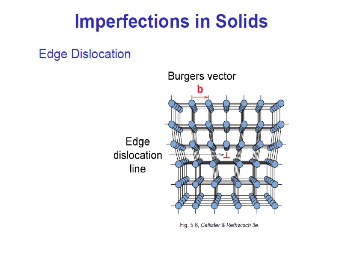
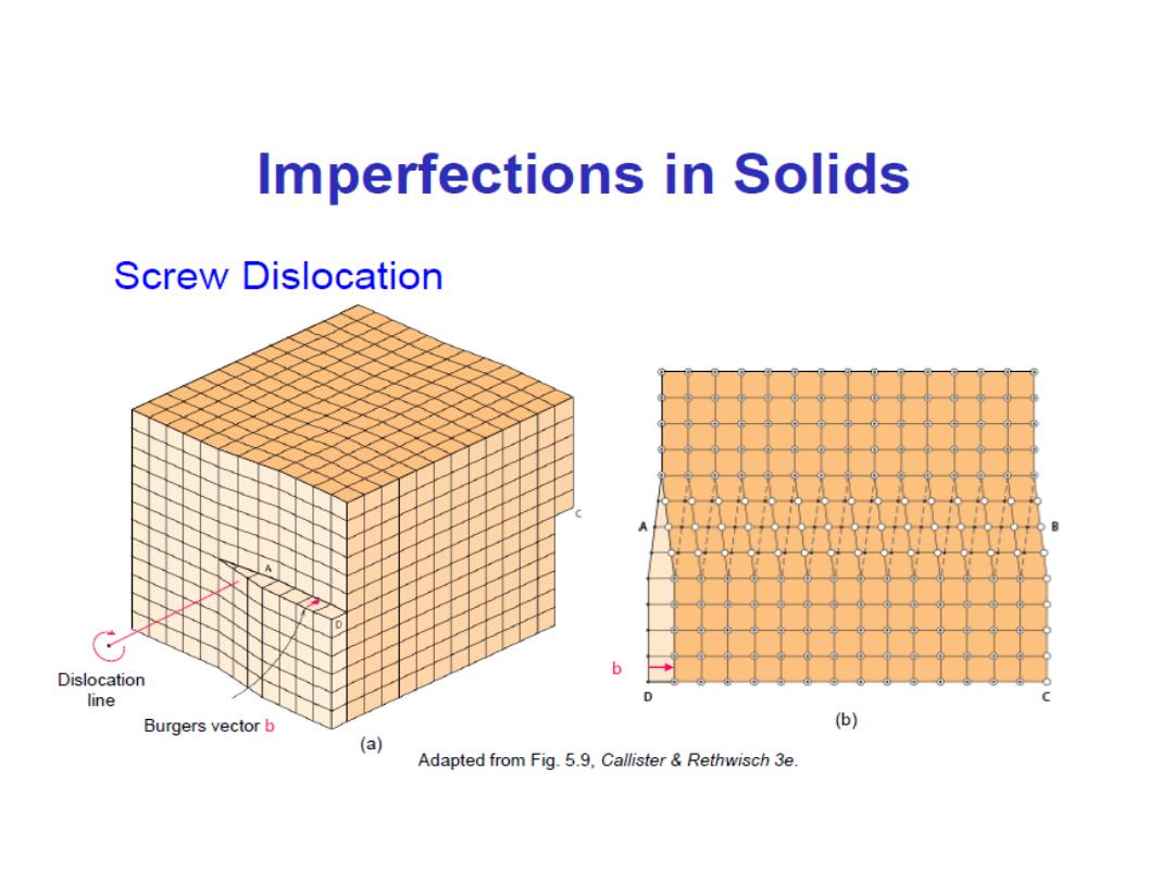
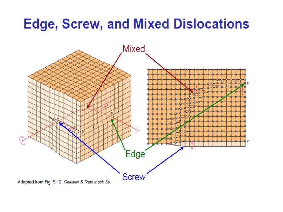
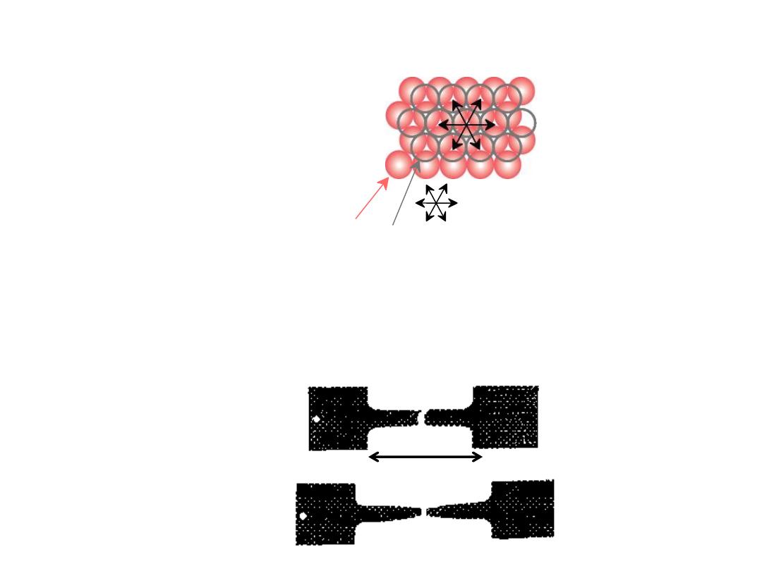
• are line defects,
• cause slip between crystal plane when they move,
• produce permanent (plastic) deformation.
Dislocations
:
Schematic of a Zinc (HCP):
• before deformation
• after tensile elongation
slip steps
LINE DEFECTS

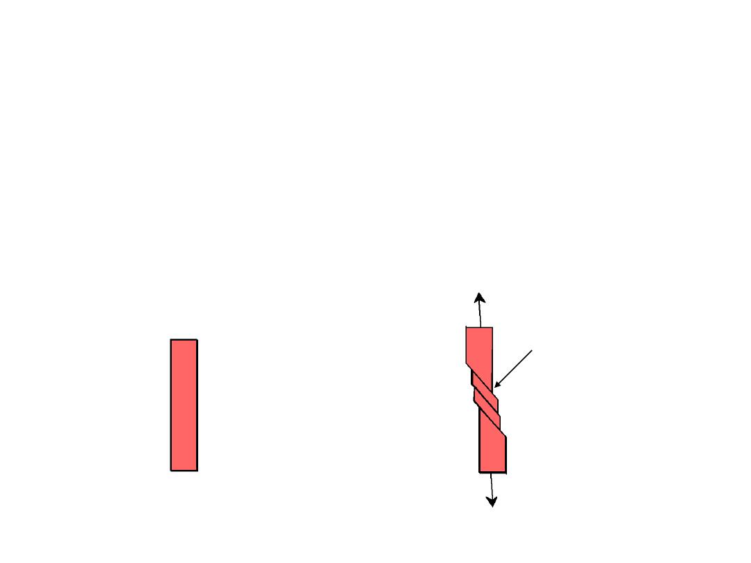
Linear Defects (
Dislocations
)
– Are one-dimensional defects around which atoms are misaligned
• Edge dislocation:
– extra half-plane of atoms inserted in a crystal structure
– b (the berger’s vector) is (perpendicular) to dislocation line
• Screw dislocation:
– spiral planar ramp resulting from shear deformation
– b is (parallel) to dislocation line
Burger’s vector, b:
is a measure of lattice distortion and is measured
as a distance along the close packed directions in the lattice
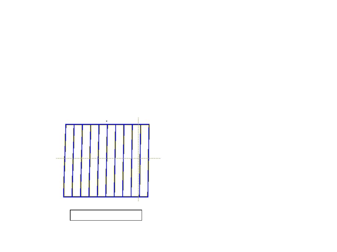
Dislocations & Crystal Structures
• Structure:
close-packed
planes & directions
are preferred.
view onto two
close-packed
planes.
close-packed plane (bottom)
close-packed plane (top)
close-packed directions
• Comparison among crystal structures:
FCC: many close-packed planes/directions;
HCP: only one plane, 3 directions;
BCC: none “super-close” many “near close”
• Specimens that
were tensile
tested.
Mg (HCP)
Al (FCC)
tensile direction
14
• Dislocations slip planes
incrementally
...
• The dislocation line (the moving red dot)...
...separates slipped material on the left
from unslipped material on the right.
Simulation of dislocation
motion from left to right
as a crystal is sheared.
(Courtesy P.M. Anderson)
INCREMENTAL SLIP
Click on image to animate
15
• Dislocation motion requires the successive bumping
of a half plane of atoms (from left to right here).
• Bonds across the slipping planes are broken and
remade in succession.
Atomic view of edge
dislocation motion from
left to right as a crystal
is sheared.
(Courtesy P.M. Anderson)
BOND BREAKING AND
REMAKING
Click on image to animate
16
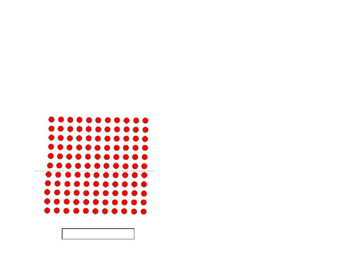
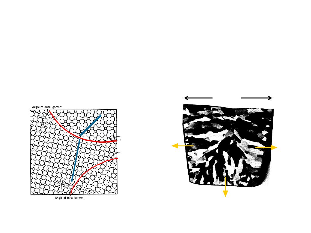
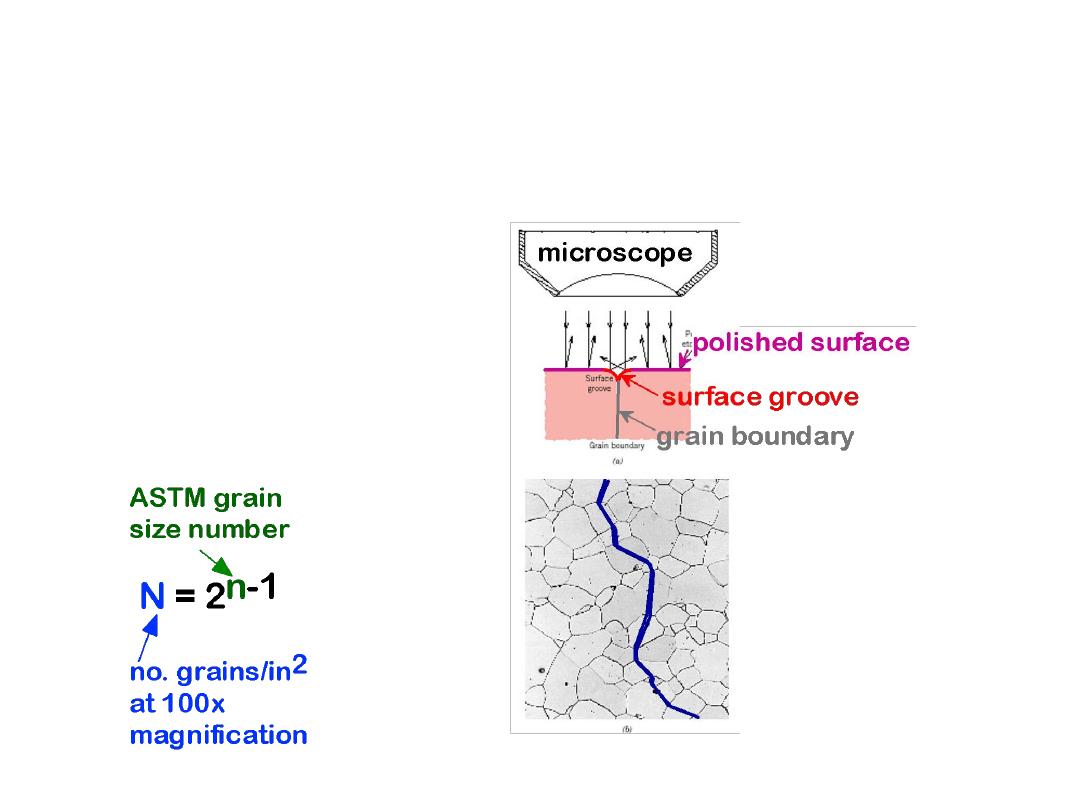
Grain boundaries
:
• are boundaries between crystals.
• are produced by the solidification process, for example.
• have a change in crystal orientation across them.
• impede dislocation motion.
grain
boundaries
heat
flow
Schematic
Adapted from Fig. 4.7,
Callister 6e.
Adapted from Fig. 4.10,
Callister 6e. (Fig.
4.10 is from
Metals Handbook, Vol. 9, 9th edition,
Metallography and Microstructures, Am. Society for
Metals, Metals Park, OH, 1985.)
~ 8cm
Metal Ingot
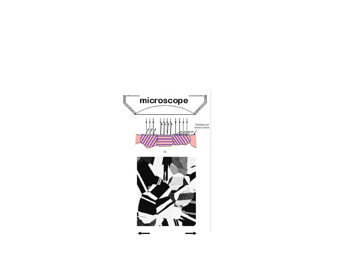
AREA DEFECTS: GRAIN
BOUNDARIES
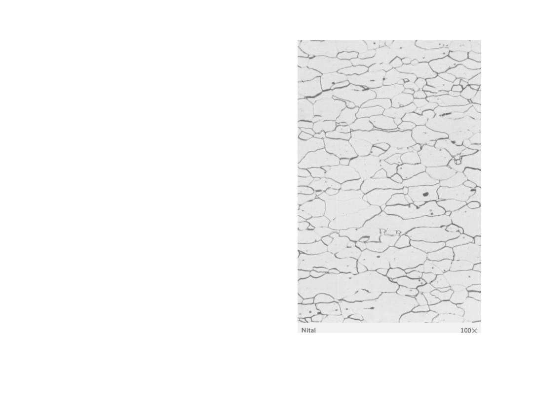
Typical optical micrograph
of a grain structure, 100
×
.
The material is a low-
carbon steel. The grain
boundaries have been
lightly etched with a
chemical solution so that
they reflect light differently
from the polished grains,
thereby giving a distinctive
contrast. (From
Metals
Handbook
, 8th ed., Vol. 7:
Atlas of Microstructures of
Industrial Alloys
, American
Society for Metals, Metals
Park, OH, 1972.)
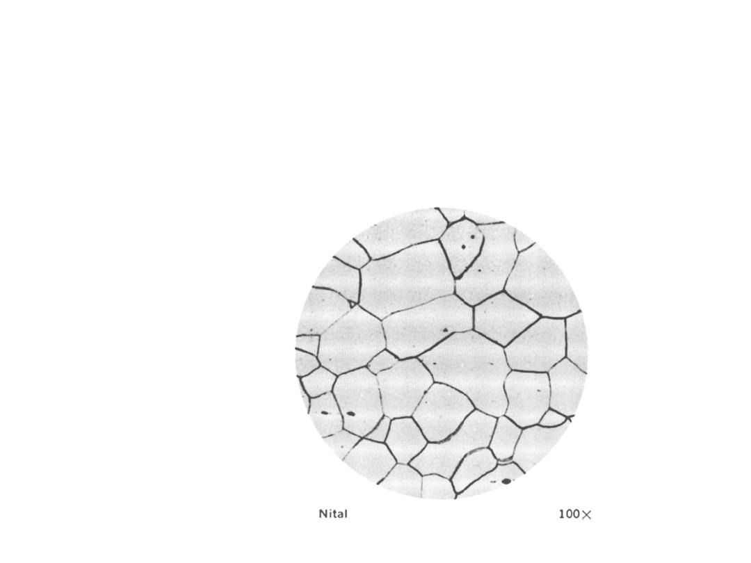
Specimen for the calculation of the grain-size number,
G is defined at a magnification of
100×
. This material
is a low-carbon steel similar to that shown in Figure
4.18. (From
Metals Handbook
, 8th ed., Vol. 7:
Atlas of
Microstructures of Industrial Alloys
, American Society
for Metals, Metals Park, OH, 1972.)
17
• Useful up to 2000X magnification.
• Polishing removes surface features (e.g., scratches)
• Etching changes reflectance, depending on crystal
orientation.
close-packed planes
micrograph of
Brass (Cu and Zn)
Adapted from Fig. 4.11(b) and (c),
Callister 6e.
(Fig. 4.11(c) is courtesy
of J.E. Burke, General Electric Co.
0.75mm
OPTICAL MICROSCOPY (1)
18
Grain boundaries...
• are imperfections,
• are more susceptible
to etching,
• may be revealed as
dark lines,
• change direction in a
polycrystal.
Adapted from Fig. 4.12(a)
and (b),
Callister 6e.
(Fig. 4.12(b) is courtesy
of L.C. Smith and C.
Brady, the National
Bureau of Standards,
Washington, DC [now the
National Institute of
Standards and
Technology, Gaithersburg,
MD].)
OPTICAL MICROSCOPY (2)
19
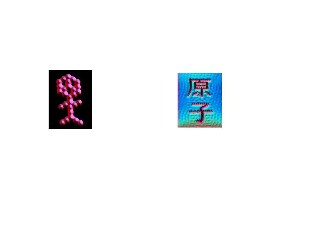
• Atoms can be arranged and imaged!
Carbon monoxide
molecules arranged
on a platinum (111)
surface.
Photos produced from
the work of C.P. Lutz,
Zeppenfeld, and D.M.
Eigler. Reprinted with
permission from
International Business
Machines Corporation,
copyright 1995.
Iron atoms
arranged on a
copper (111)
surface. These
Kanji characters
represent the word
“atom”.
SCANNING TUNNELING
MICROSCOPY
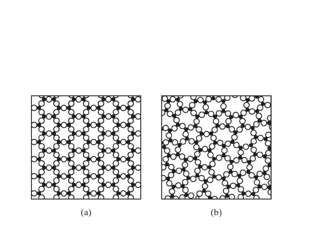
Two-dimensional schematics give a comparison of (a)
a crystalline oxide and (b) a non-crystalline oxide. The
non-crystalline material retains short-range order (the
triangularly coordinated building block), but loses
long-range order (crystallinity). This illustration was
also used to define glass in Chapter 1 (Figure 1.8).
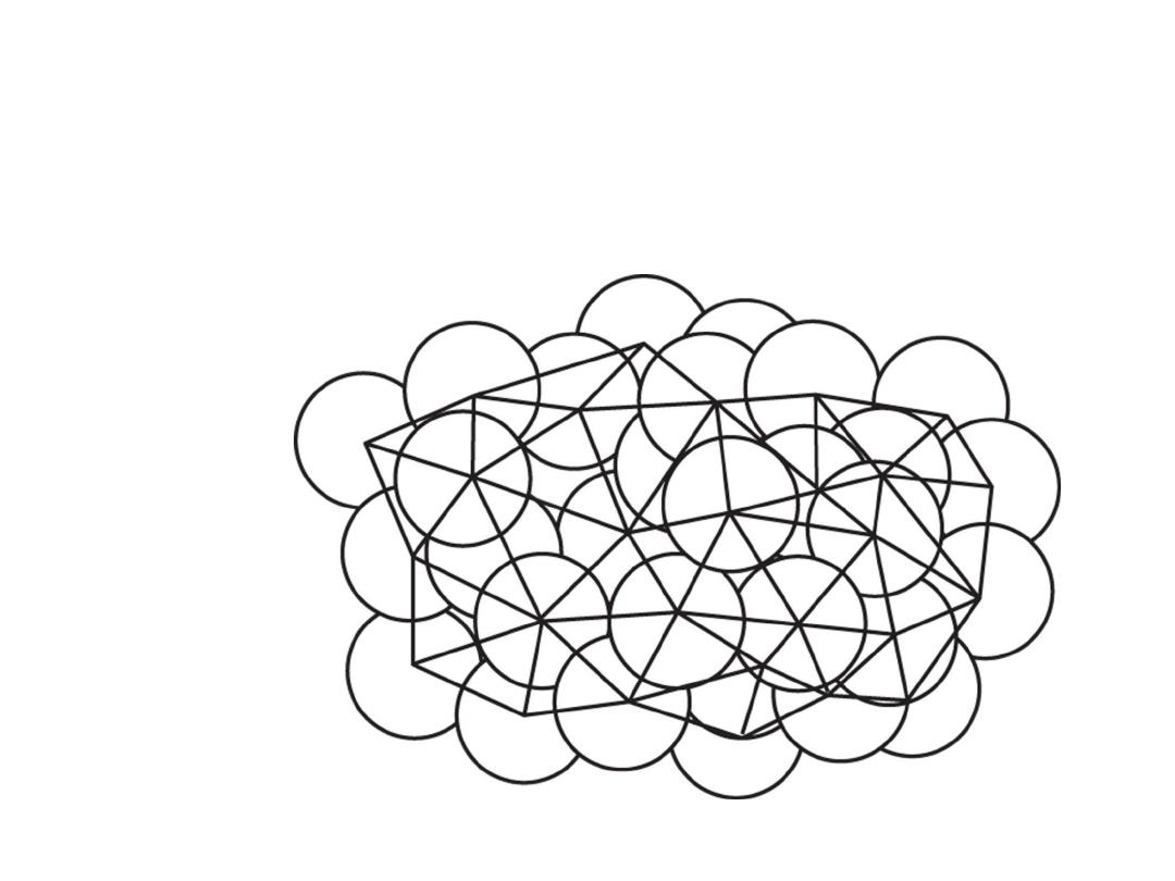
Bernal model of an amorphous metal structure. The
irregular stacking of atoms is represented as a
connected set of polyhedra. Each polyhedron is
produced by drawing lines between the centers of
adjacent atoms. Such polyhedra are irregular in shape
and the stacking is not repetitive.
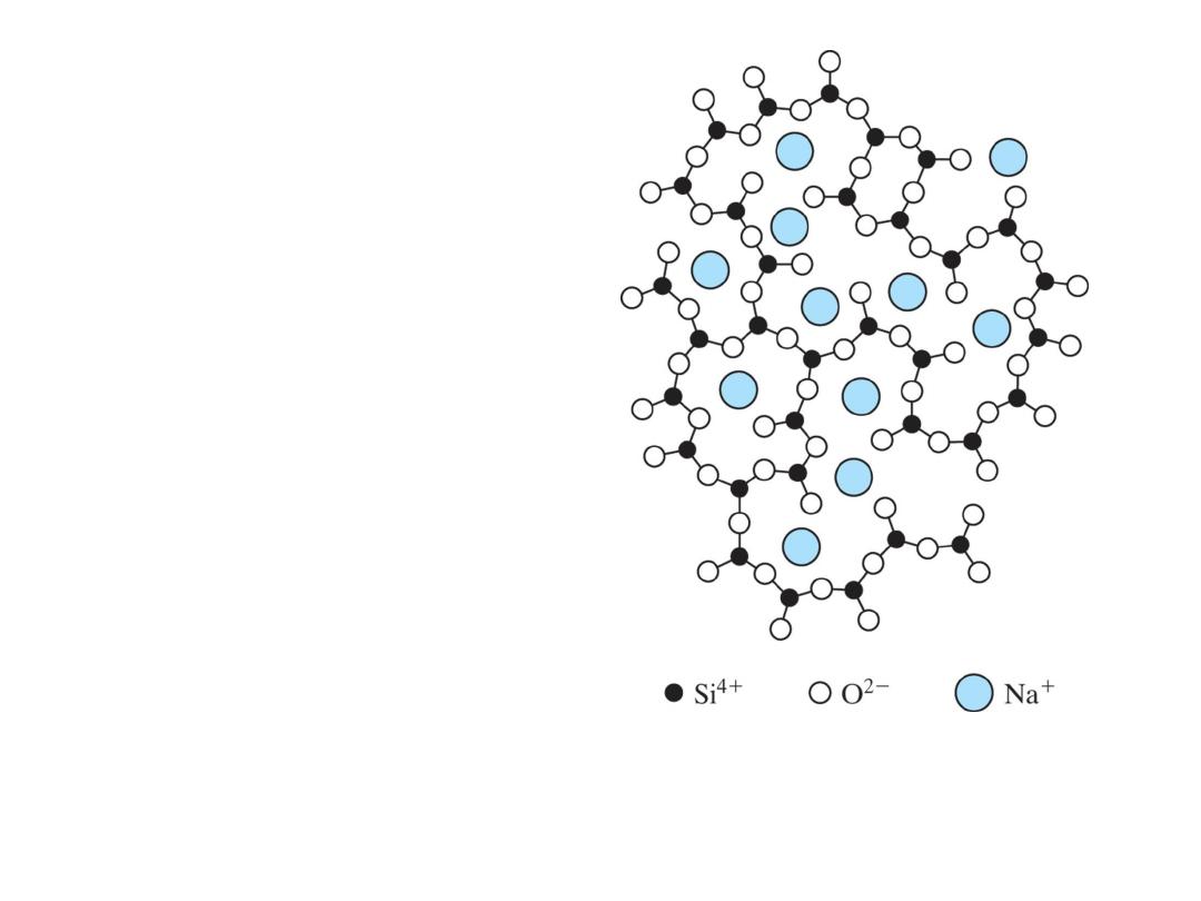
A chemical impurity such
as Na
+
is a glass modifier,
breaking up the random
network and leaving
nonbridging oxygen ions.
[From B. E. Warren,
J. Am.
Ceram. Soc. 24
, 256
(1941).]
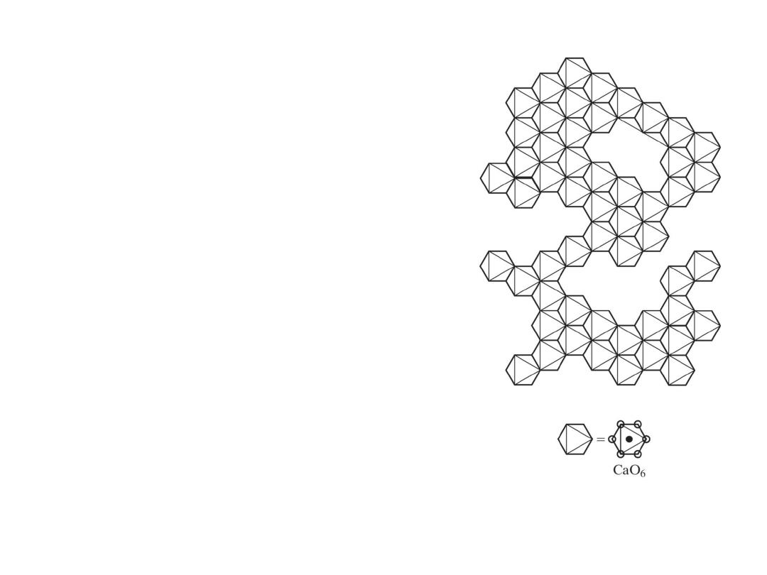
Schematic illustration of
medium-range ordering in a
CaO–SiO
2
glass. Edge-sharing
CaO
6
octahedra have been
identified by neutron-diffraction
experiments. [From P. H. Gaskell
et al.,
Nature 350
, 675 (1991).]

Summary
• Point
,
Line
,
Surface
and
Volumetric
defects exist in solids.
• The number and type of defects can be varied and
controlled
– T controls vacancy conc.
– amount of plastic deformation controls # of dislocations
– Weight of charge materials determine concentration of
substitutional or interstitial point ‘defects’
• Defects affect material properties (e.g., grain boundaries
control crystal slip).
• Defects may be desirable or undesirable
– e.g., dislocations may be good or bad, depending on whether
plastic deformation is desirable or not.
– Inclusions can be intention for alloy development