
Chapter 4
Diodes and their applications
—————————————————————————————————–
If one side of a piece of silicon dope with a trivalent impurity and the
other side with a pentavalent impurity, a (p − n) junction will formed be-
tween the resulting p-type and n-type portions and a basic diode will cre-
ated. A diode is a device that conducts current in only one direction. In
this chapter we demonstrate the characteristics of the (p − n) junction re-
gion. The volt-ampere characteristics of the (p−n) junction is studied. The
capacitance across the junction is calculated.
——————————————————————————————————
4.1
Introduction
Several common physical configurations of diodes are illustrated in Figure 4.1. The
anode and cathode are indicated on a diode in several ways, depending on the type of
package. The cathode is usually marked by a band, a tab, or some other feature. On
those packages where one lead is connected to the case, the case is the cathode.
Summary of diode biasing:
Forward bias:
• Bias voltage connections: positive to (p) region: negative to (n) region.
• The bias voltage must be greater than the barrier potential.

64
Diodes and their applications
Figure 4.1: Typical diode packages with terminal identification.
• Majority carriers flow toward the (pn) junction.
• Majority carriers provide the forward Current.
• The depletion region narrows.
Reverse bias:
• Bias voltage connections: positive to (n) region; negative to (p) region.
• The bias voltage must be less than the breakdown voltage.
• Majority carriers flow away from the (pn) junction during short transition time.
• Minority carriers provide the extremely small reverse current.
• There is no majority carrier current after transition time.
• The depletion region widens.
4.2
The diode model
There are three models of the diode:
4.2.1
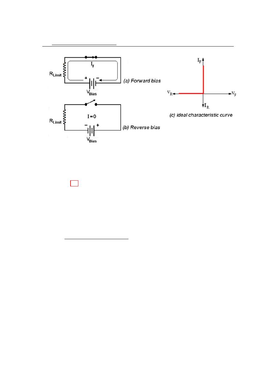
The ideal model
The ideal model of a diode is a simple switch. When the diode is forward biased,
it acts like closed (on) switch, as shown in figure 4.2a. When the diode is reversed
biased. It acts like an open (of f ) switch, as shown figure 4.2b. The barrier potential,
the forward dynamic resistance, and the reverse current are all neglected.
4.2
The diode model
65
Figure 4.2: The ideal model of the diode (a) forward bias, (b) reverse bias and (c) ideal
characteristic curve.
In figure 4.2c, the ideal V − I characteristic curve graphically depicts the ideal diode
operation.
In the ideal diode model: V
F
= 0, I
R
= 0 and V
R
= V
bias
.
4.2.2
The practical model
The practical model adds the barrier potential to the ideal switch model. When
the diode is forward biased, it is equivalent to a closed switch in series with a small
equivalent voltage source equal to the barrier potential with the positive side toward
the anode, as indicated in figure3a. This equivalent voltage source represents the fixed
voltage drop (V
F
) produced across the forward biased (p − n) junction of the diode and
is not an active source of voltage. This voltage (V
F
) consists of the barrier potential
voltage (V
o
) plus the small voltage drop across dynamic resistance of the diode (r
d
), as
indicated by the portion of the curve to the right of the origin. The curve slopes because
the voltage drops due to dynamic (r
d
) as the current increases.
66
Diodes and their applications
Figure 4.3: The complete model of the diode (a) forward bias, (b) reverse bias and (c)
ideal characteristic curve (silicon).
4.2.3
The complete model
For the complete model of a silicon diode, the following formulas apply:
V
F
= V
o
+ I
F
× r
d
I
F
=
(V
Bias
− V
o
)
(R
Limit
+ r
d
)
The reverse current is taken into account with the parallel resistance and is indicated
by the portion of the curve to the left of the origin.
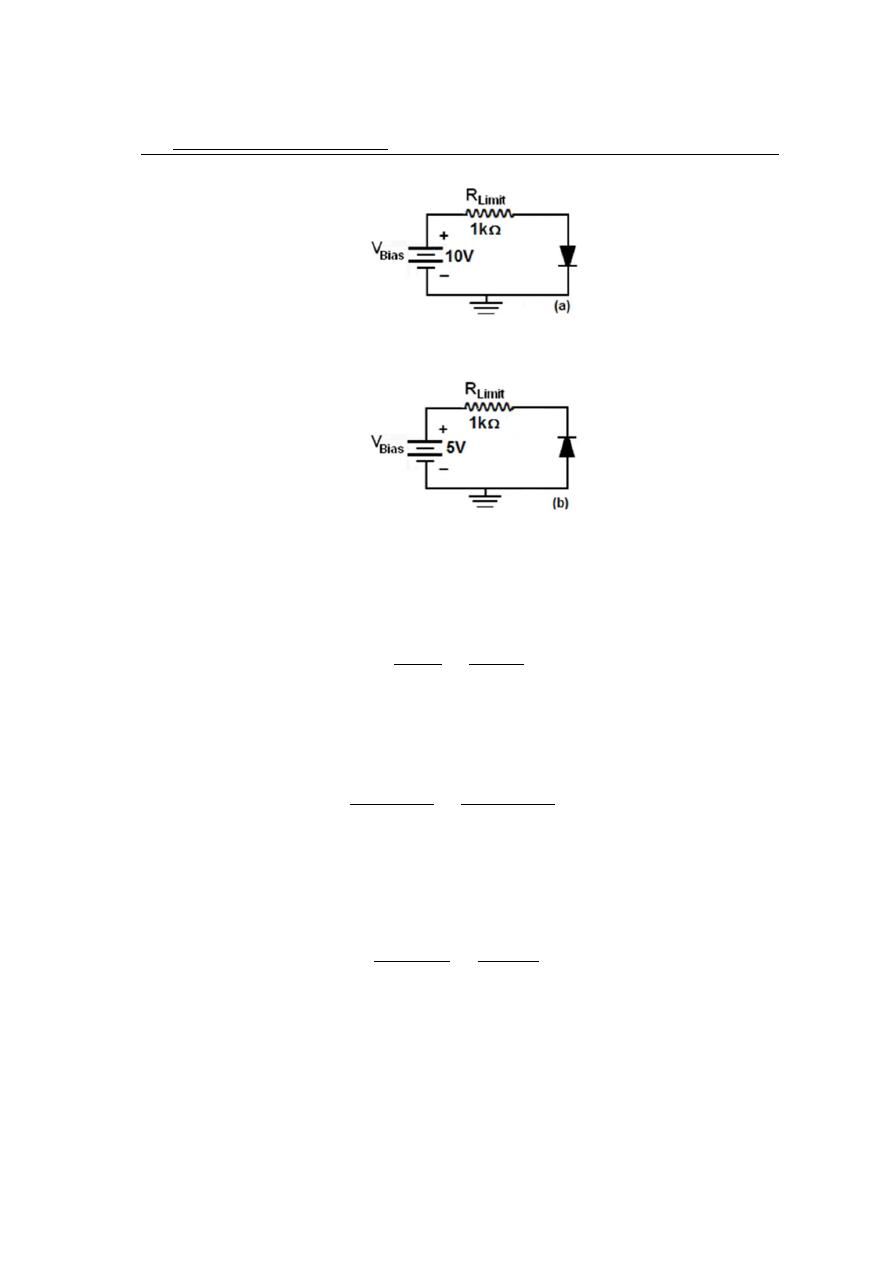
Solved problem
a) Determine the forward voltage and forward current for the diode in figure (a) for
each of the diode models. Also find the voltage across the limiting resistor in each case.
Assume r
d
= 10Ω at the determined value of forward current.
b) Determine the reverse voltage and reverse current for the diode in figure (b) for
each of the diode models. Also find the voltage across the limiting resistor in each case.
Assume I
R
=1µA.
Solution:
4.2
The diode model
67
Figure 4.4:
Figure 4.5:
a) Ideal model:
V
F
= 0 volt
I
F
=
V
bias
R
Limit
=
10
1 × 10
3
= 10 mA
V
R
limit
= I
F
× R
Limit
= 10 mA × 1kΩ = 10 volt
Practical model:
V
F
= 0.7 volt
I
F
=
V
bias
− V
F
R
Limit
+ r
d
=
10 − 0.7
1 × 10
3
+ 10
= 9.21 mA
V
d
= 0.7 + I
F
× r
d
= 0.7 + 9.21mA × 10 = 792mV
V
R
limit
= I
F
× R
Limit
= 9.21 mA × 1kΩ = 9.21 volt
If we neglected r
d
then;
I
F
=
V
bias
− V
F
R
Limit
=
10 − 0.7
1 × 10
3
= 9.3 mA
V
R
limit
= I
F
× R
Limit
= 9.3 mA × 1kΩ = 9.3 volt
b) Ideal model:
I
R
= 0 A
68
Diodes and their applications
V
R
= V Bias = 5 V
V
R
limit
= 0 volt
Practical model
I
R
= 1 µA
V
R(limit)
= I
R
× R
(
Limit) = 1µA × 1kΩ = 1mV
V
R
= V
(
Bias) − V
R
(
limit)=5V −1mV =4.999 volt
4.3
Diode Applications
Because of their ability to conduct current in one direction and block current in the
other direction, diodes are used in circuits called rectifiers that convert ac voltage into
dc voltage. Rectifiers are found in all dc power supplies that operate from an ac voltage
source. A power supply is an essential part of each electronic system from the simplest
to the most complex. In this section, you will study the most basic type of rectifiers,
the half-wave rectifier, full-wave rectifiers and power supply filters and regulators, and
the diode limiting and clamping circuits, and voltage multipliers.
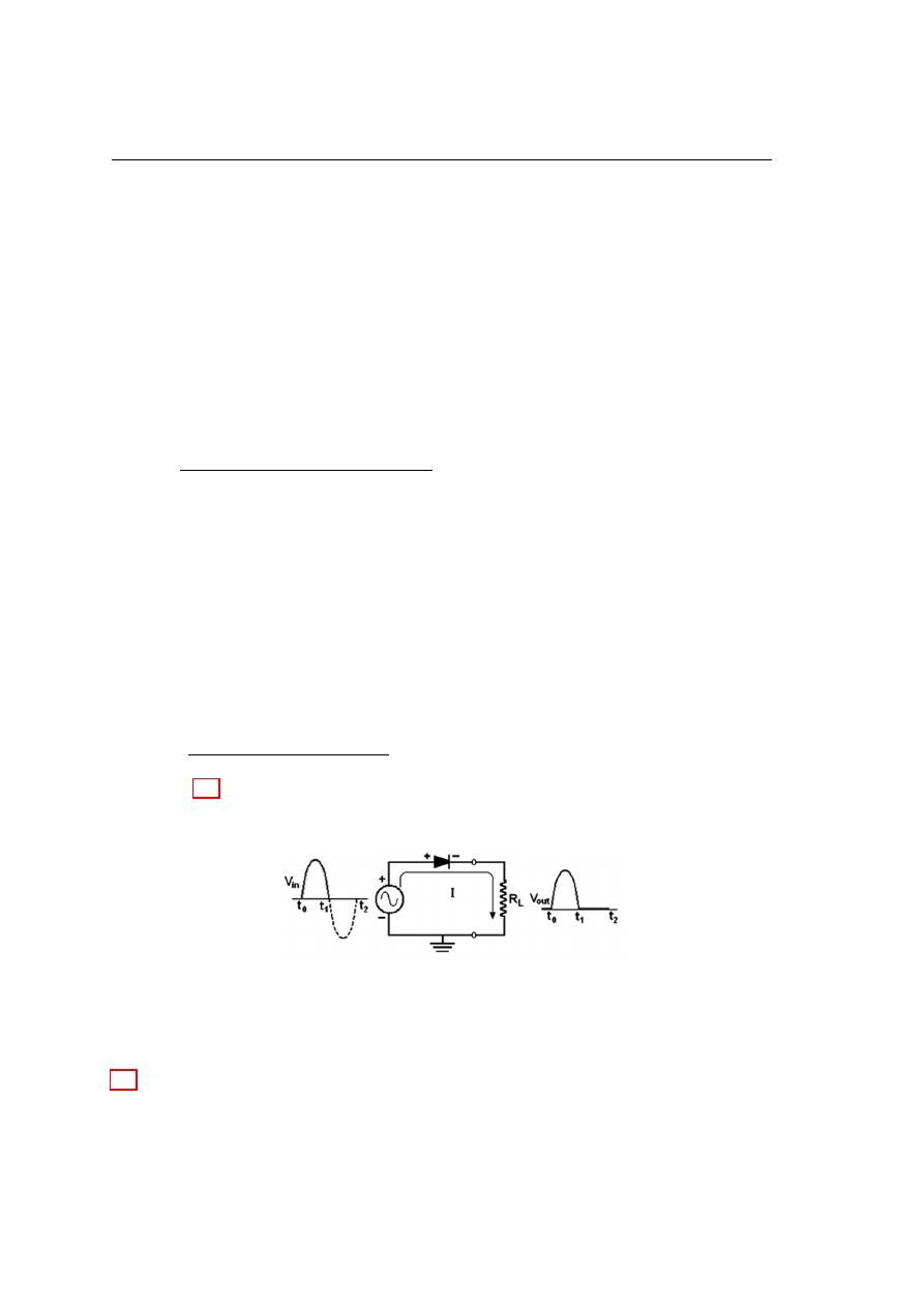
4.3.1
Half-wave rectifier
Figure 4.6, illustrates the process called half wave rectification. The diode connection
to an ac source and to a load resistor R
L
will form a half-wave rectifier. When the input
Figure 4.6: Half-wave rectifier circuit with the input and output voltage waveform.
voltage (V
i
n) goes positive during the time duration between t
0
to t
1
, as shown in Figure
4.6, the diode will biased forward and conducts current through the load resistor. The
current produces an output voltage across the load R
L
which has the same shape as
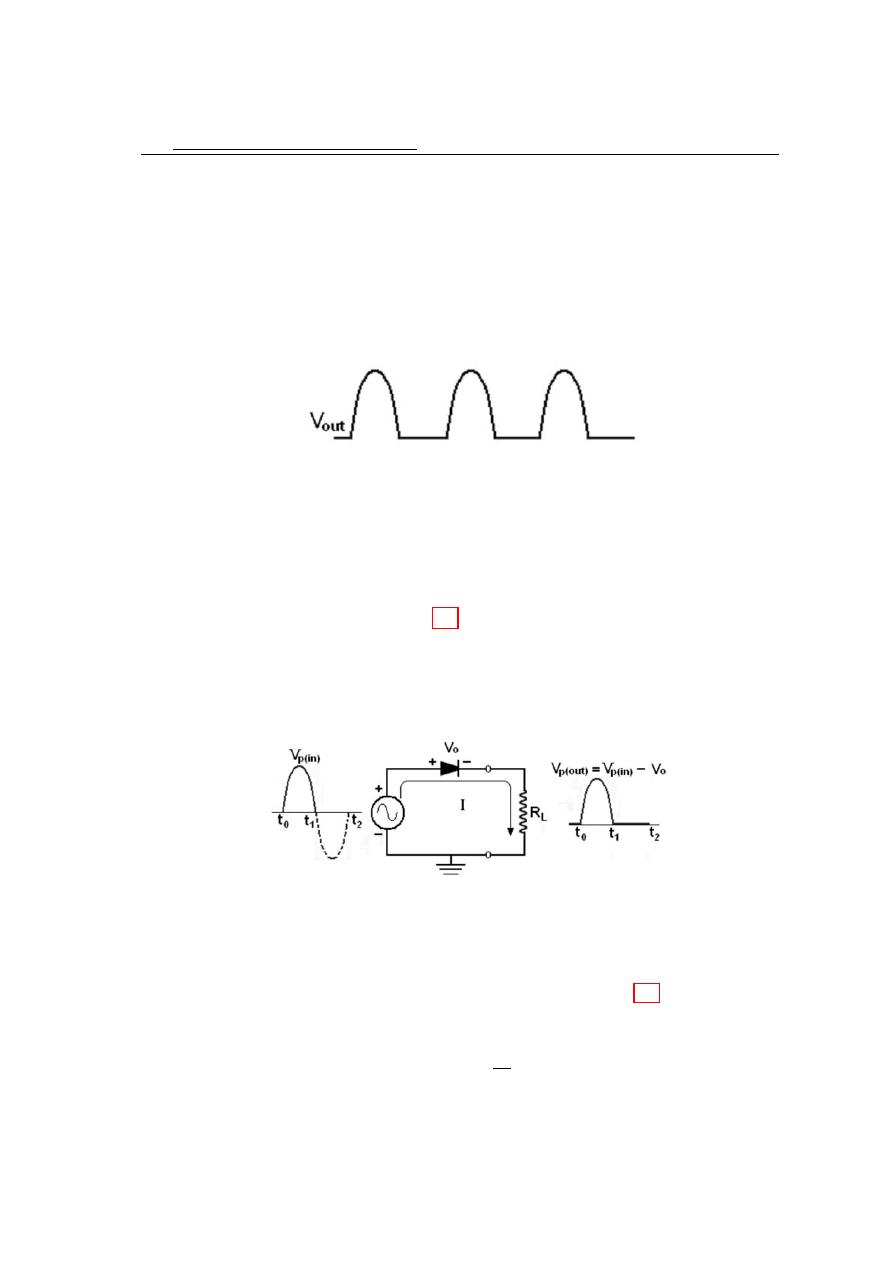
4.3
Diode Applications
69
the positive half cycle of the input voltage. As the input voltage goes negative, during
the second half of the input voltage cycle (t
1
to t
2
), the diode will biased reverse. As
a result there is no current will pass through the load R
L
and the voltage across the
load resistor is 0 V . The net result is that only the positive half cycles of the ac input
voltage appear across the load as shown in Figure 5. Since the output does not change
polarity, it is a pulse dc voltage. When the practical diode model is used with the
Figure 4.7: Half-wave output voltage for three input cycles.
barrier potential of (V
o
) taken into account. During the positive half cycle, the input
voltage must overcome the barrier potential before the diode becomes forward biased.
This result in a half wave output with a peak value that is less than the peak value of
the input by (V
o
), as shown in Figure 4.8.
V
p(out)
= V
p(in)
− V
o
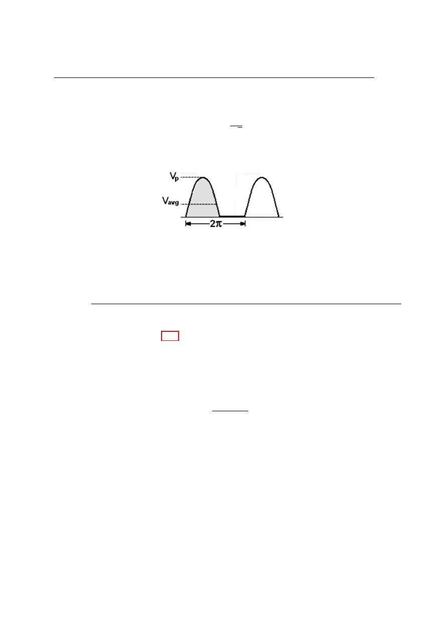
The mean value of the output voltage (V
avg
or V
dc
) can be calculated mathematically
Figure 4.8: The effect of the barrier potential on the half wave rectified output voltage
is to reduce the peak value of the input by V
o
.
by the area under the curve over a full cycle, as shown in Figure 4.9 dividing by 2π, the
number of radians in a full cycle, where V
p
is the peak value of the voltage.
V
avg
=
V
p
π
70
Diodes and their applications
The root mean square value of the output voltage (V
rms
) is given as:
V
rms
=
V
p
√
2
Figure 4.9: Average value of the half wave rectified signal.
4.3.5
Half wave rectifier with transformer coupled input voltage
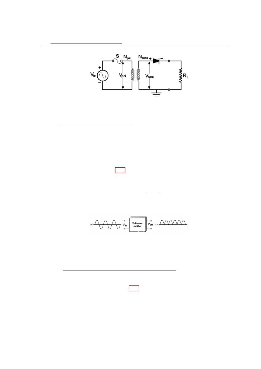
A transformer is often used to couple the ac input voltage from the source to the
rectifier, as shown in figure 4.10. Transformer coupling provides two advantages: 1. It
allows the source voltage to be stepped up or stepped down as needed. 2. The ac source
is electrically isolated from the rectifier, thus preventing a shock hazard in the secondary
circuit. The turn’s ratio (n) is equal to the ratio of secondary turns (N
secondary
) to the
primary turns (N
primary
):
n =
N
secondary
N
primary
N
secondary
= n × N
primary
If n > 1, the secondary voltage is greater than the primary voltage. If n < 1, the sec-
ondary voltage is less than the primary voltage. The peak secondary voltage, V
p(secondary)
in a transformer coupled half wave rectifier is equal to V p(in). Therefore:
V
p(out)
= V
p(secondary)
− V
o
4.4
Full Wave Rectifier
71
Figure 4.10: Half wave rectifier with transformer coupled input voltage.
4.4
Full Wave Rectifier
A full-wave rectifier allows unidirectional (one-way) current through the load during
the entire 360
o
of the input cycle, whereas a half-wave rectifier allow current through
the load only during one-half of the cycle. The result of full-wave rectification is an
output voltage with a frequency twice the input frequency that pulsate every half-cycle
of the input, as shown in Figure 4.11. The average or dc value for a full wave rectified
sinusoidal voltage is twice that of the half wave, as shown in the following formula:
V
dc
= V
avg
=
2 × V
p
π
V
a
vg is approximately 63.7% of V
P
for a full wave rectifiered voltage.
Figure 4.11: Full wave rectifier.
4.6.1
The centre tapped full wave rectifier
A centre tapped rectifier use two diodes connected to the secondary of a center
tapped transformer as shown in figure 4.12. The input voltage is coupled through the
transformer to the centre tapped secondary. Half of the total secondary voltage appears
between the center tap and each end of the secondary winding as shown. For a positive
half cycle of the input voltage, the polarities of the secondary voltages are as shown in
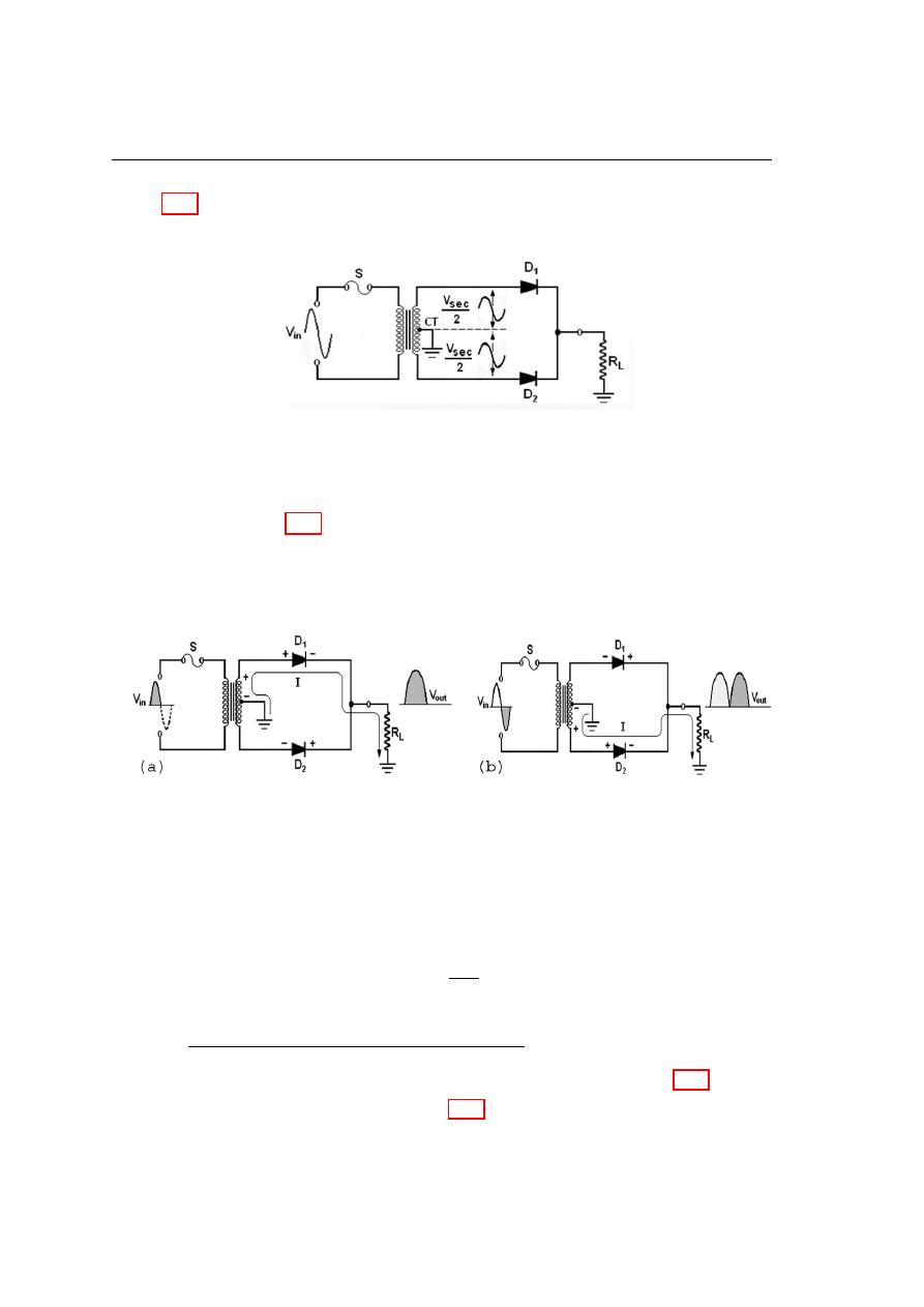
72
Diodes and their applications
figure 4.13(a). This condition forward biases diode D
1
and reverse biases diode D
2
.
The current path is through D
1
and the load resistor R
L
as indicated.
Figure 4.12: A centre-tapped full-wave rectifier.
For a negative half cycle of the input voltage, the voltage polarities on the secondary
are as shown in figure 4.13(b). This condition reverses biases D
1
and forward biases D
2
.
The current path is through D
2
and R
L
as indicated. Because the output current during
through the load, the output voltage developed across the load resistor is a full wave
rectified dc voltage as shown. The output voltage of a center tapped full wave rectifier
Figure 4.13: Basic operation of a centre tapped full wave rectifier. a) During positive
half cycles, D
1
is forward biased and D
2
is reverse biased. b) During negative half cycles.
D
2
is forward-biased and D
1
is reverse biased.
is always one half of the total secondary voltage less the diode drop, no matter what
is the turn’s ratio.
V
out
=
V
sec
2
− V
o
4.6.8
The Bridge Full wave Rectifier
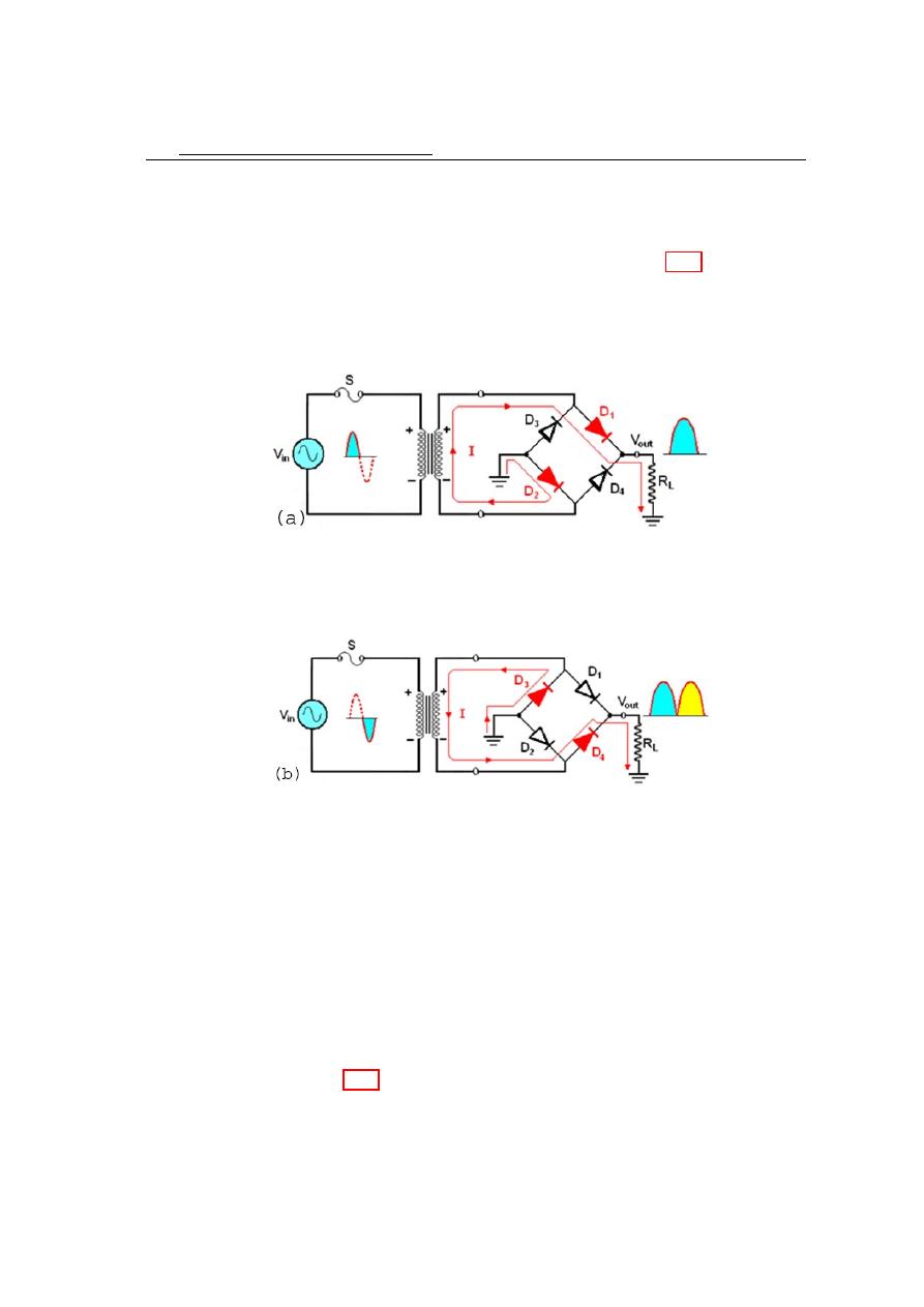
The bridge rectifier uses four diodes connected as shown in figure 4.14. When the
input cycle is positive, as shown in figure 4.14a, diodes D
1
and D
2
are forward biased
4.4
Full Wave Rectifier
73
and conduct current in the direction shown by arrow. A voltage is developed across R
L
that looks like the positive half of the input cycle. During this time, diodes D
3
and D
4
are reverse biased. When the input cycle is negative as in figure 4.15b, diodes D
3
and
D
4
are forward biased and conduct current in the same direction through R
L
as during
the positive half cycle. During the negative half cycle, D
1
and D
2
are reverse biased. A
full wave rectified output voltage appears across R
L
as a result of this action. Bridge
Figure 4.14: Figure 12(a) During the positive half cycle of the input. D
1
and D
2
are
forward biased and conduct current D
3
and D
4
are reverse biased.
Figure 4.15: Figure 12(b) During the negative half cycle of the input. D
3
and D
4
are
forward biased and conduct current while D
1
and D
2
are reverse biased.
output voltage:
During the positive half cycle of the total secondary voltage, diodes D
1
and D
2
are
forward biased. Neglecting the diode drops, the secondary voltage appears across the
load resistor. The same is true when D
3
and D
4
are forward biased during the negative
half cycle.
V
p(out)
= V
p(sec)
It can be seen in figure 4.16. Two diodes are always in series with the load resistor
during both the positive and negative half cycles. If these diode drops are taken into
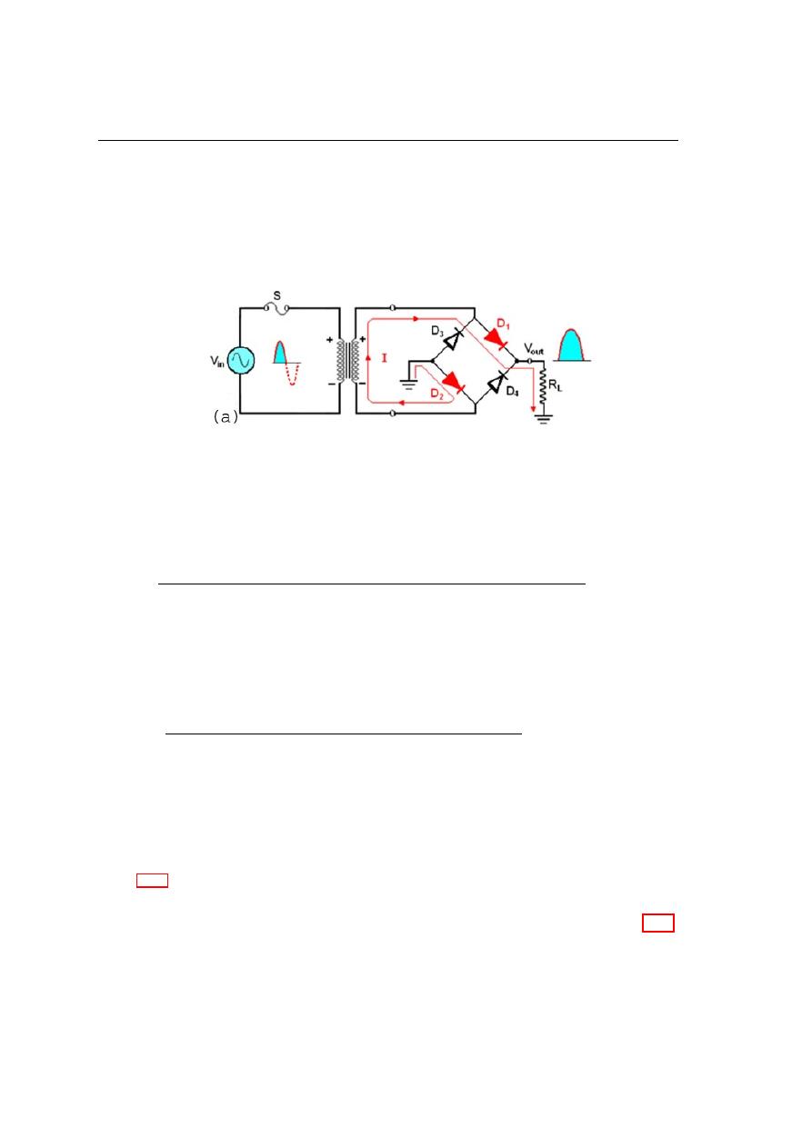
74
Diodes and their applications
account, the output voltage is:
V
p(out)
= V
p(sec)
− V
o
Figure 4.16: Bridge operation during a positive half cycle of the primary and secondary
voltages.
4.7
Power Supply Filters and Regulators
In the most power supply applications, the standard 50 Hz AC power line voltage
should be converted to an approximately constant DC voltage. The pulsating DC output
of a rectifier must be filtered to reduce the large voltage variations.
4.9.1
Power Supply Filters and Regulators
The filter is simply a capacitor connected from the rectifier output to ground. R
L
represents the equivalent resistance of a load.
1. During the positive first quarter cycle of the input, the diode is forward biased,
allowing the capacitor to charge to within V
o
of the input peak, as shown in figure
2. When the input begins to decrease below its peak. As shown in figure 4.18, the
capacitor retains its charge and the diode becomes reverse biased because the
cathode is more positive than the anode. During the remaining part of the cycle,
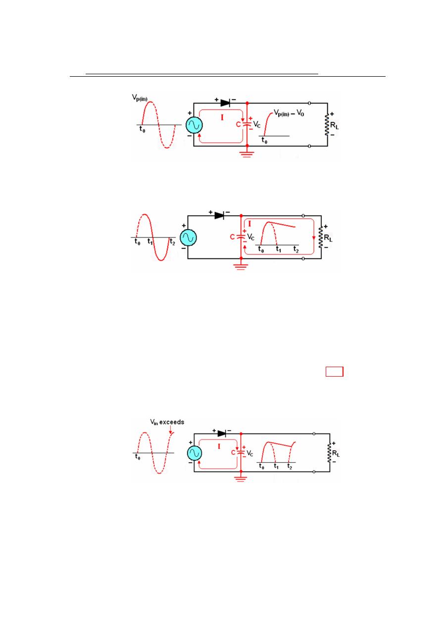
4.7
Power Supply Filters and Regulators
75
Figure 4.17: Initial charging of the capacitor (diode is forward biased) happens only
once when power is turned on.
Figure 4.18: The capacitor discharges through R
L
after peak of positive alternation
when the diode is reverse biased.
the capacitor can discharge only through the load resistance at a rate determined
by the R
L
C time constant.
3. During the first quarter of the next cycle, as shown in figure 4.19, the diode will
again become forward biased when the input voltage exceeds the capacitor voltage
by approximately V
o
.
Figure 4.19: The capacitor charges back to peak of input when the diode becomes
forward-biased.
76
Diodes and their applications
4.9.2
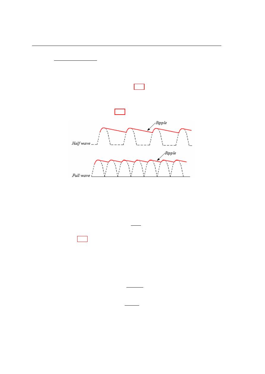
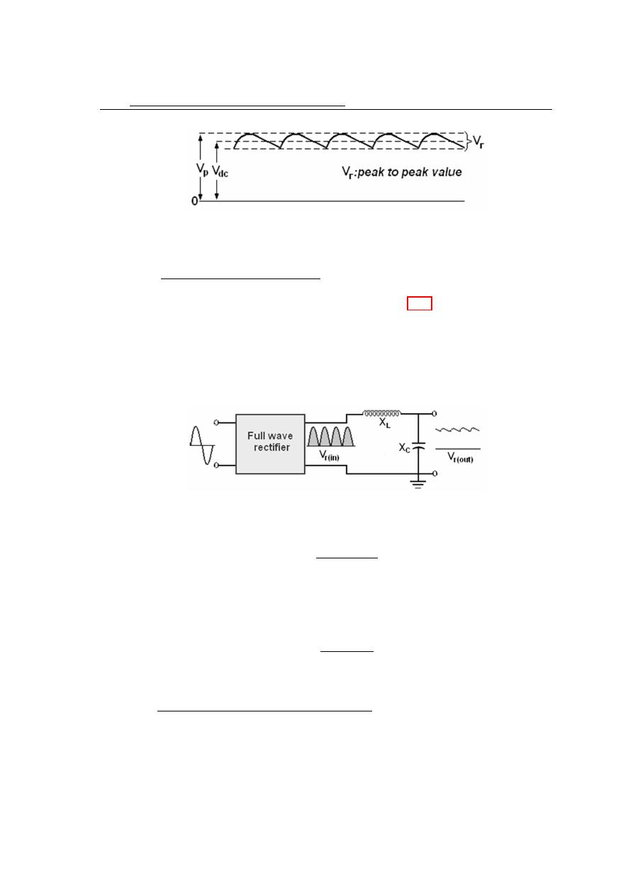
Ripple Factor
The variation in the capacitor voltage due to the charging and discharging is called
the ripple voltage. Generally, ripple is undesirable; thus, the smaller the ripple, the
better the filtering action, as shown in figure 4.20. When filtered, the full wave rectified
voltage has a smaller ripple than does a half wave voltage for the same load resistance
and capacitor values. The capacitor discharges less during the shorter interval between
full-wave pulses, as shown in figure 4.20a and b. The ripple factor is an indication of
Figure 4.20: Comparison of ripple voltages for (a) half wave and (b) full wave rectified
voltages with the same filter capacitor and load.
the effectiveness of the filter and is defined as:
r =
V
rms
V
dc
As shown in figure 4.21. The ripple factor can be lowered by increasing the value of
the filter capacitor or increasing the load resistance. For a full wave rectifier with a
capacitor input filter, approximations for the peak to peak ripple voltage, V
rms
and the
DC value of the filter output voltage is V
d.c
, are given in the following expressions. The
variable V
p(rect)
is the unfiltered peak rectified voltage.
V
dc
=
1 −
0.00417
R
L
C
V
p(rect)
V
rms
=
0.0024
R
L
C
V
p(rect)
The last formulas are for ripple filtered signal.
4.12
Diode Clipping Circuits
77
Figure 4.21: V
rms
and V
dc
determination for the ripple factor calculation
4.10.3
Inductor Input Filter
When a choke is add to the filter input, as in figure 4.22, a reduction in the ripple
voltage V
rms
is achieved. The choke has a high reactance at the ripple frequency. The
capacitive reactance is low compared to both R
L
and X
L
(10 time at least).
The
magnitude of the out ripple voltage of the filter is determined with voltage divider
equation:
Figure 4.22: The LC filter as it look to the AC component.
V
rms(out)
=
X
C
|X
L
− X
C
|
V
rms(in)
Since the choke presents a winding resistance R
w
in series with load resistance R
L
.
This resistance produce undesirable reduction of DC value, therefore R
w
must be small
compared of R
L
.
V
dc(out)
=
R
L
R
L
− R
w
V
dc(in)
4.12
Diode Clipping Circuits
Diode circuits, called limiters or clippers, are sometimes used to clip off portions
of signal voltages above or below certain levels. Another type of diode circuit, called
78
Diodes and their applications
a clamper, is used to add or restore a DC level to an electrical signal. In the present
lecture we will discuss the clipping circuits only.
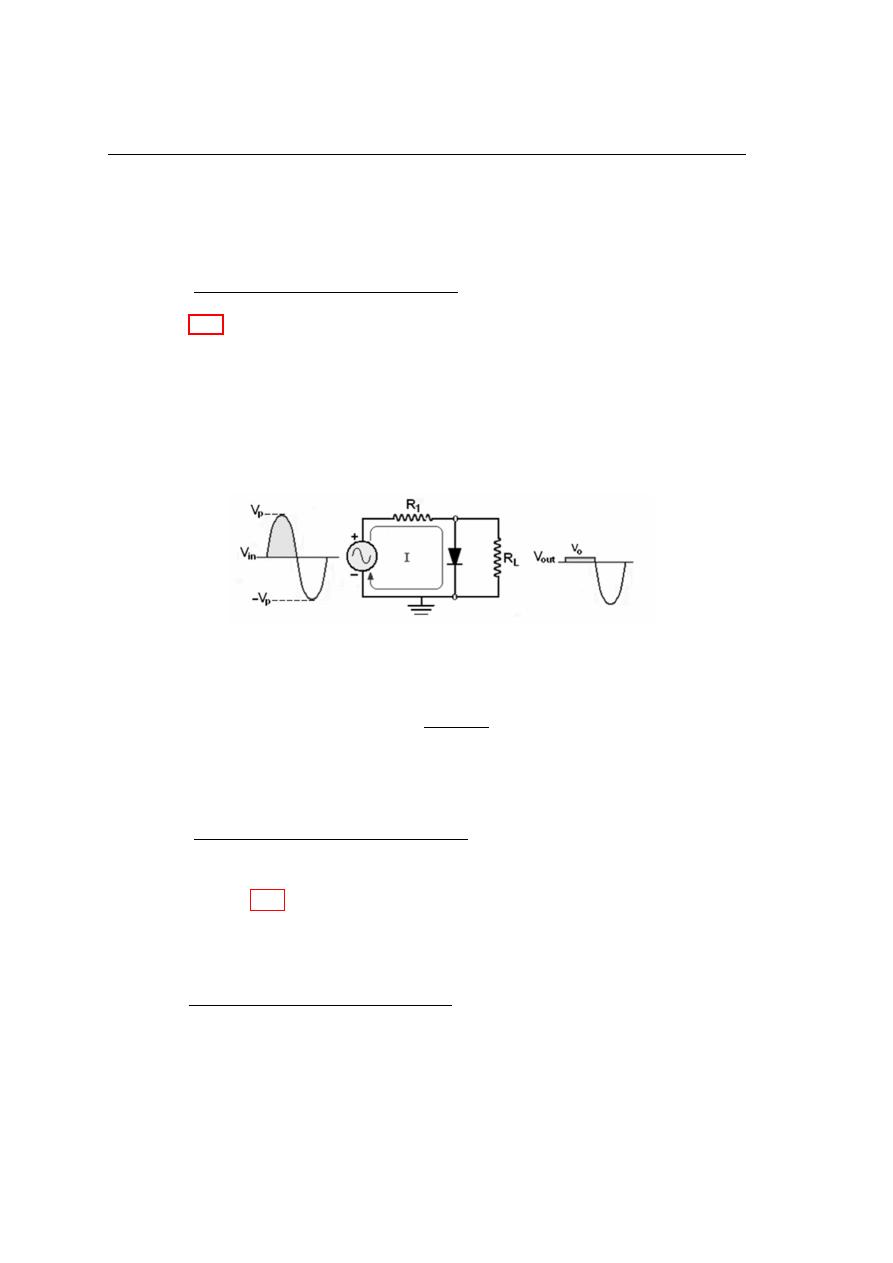
4.12.1
Positive Clipping Circuit
Figure 4.23 shows a diode clipper that clips the positive part of the input voltage.
As the input voltage goes positive, the diode becomes forward biased and conducts the
current. So point A is limited to (+ V
o
), when the input go back below V
o
, the diode is
reverse biased and appears as an open the output voltage is look like the negative part
of the input voltage, but with magnitude determined by the voltage divider formed by
R
1
and the load resistance R
L
, as follow:
Figure 4.23: Circuit for the positive clipper.
V
out
=
R
L
R
L
+ R
1
V
in
if R
1
is much less than R
L
⇒ V
out
≈ V
in
4.13.2
Negative Clipping Circuit
To obtain negative biased clipper circuit, the diode and bias voltage must connect
as shown in figure 4.24. In this case, the voltage at point A must go below (−V
B
− V
o
)
to forward bias the diode an initiate limiting action as shown.
4.15
Voltage Divider Bias
The bias voltage sources that have been used to explain the basic operation of diode
limiter can be replaced by a resistive voltage divider that derives the desired bias voltage
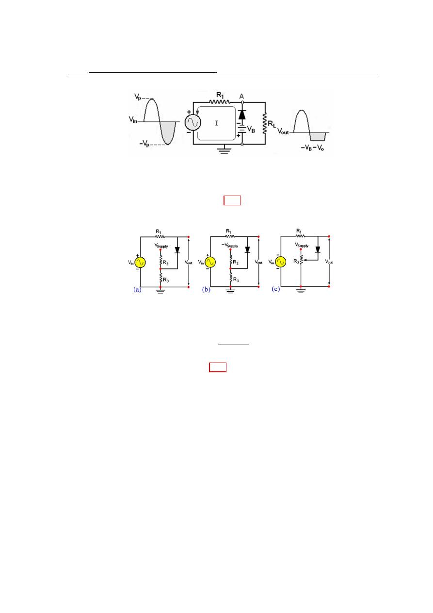
4.15
Voltage Divider Bias
79
Figure 4.24: Circuit for the negative clipper.
from the dc supply voltage, as shown in 4.25. The bias voltage is set by the resistor
values according to the voltage divider formula.
Figure 4.25: Circuit for the negative clipper.
V
Bias
=
R
3
R
2
+ R
3
V
supply
A positively biased limiter is shown in 4.25a, a negatively biased limiter is shown in part
(b), and a variable positive bias circuit using a potentiometer voltage divider is shown in
part (c). The bias resistors must be small compared to (R), so that the forward current
through the diode will not affect the bias voltage.