Experiment (4): Common Emitter Amplification Circuit
1
2016-2017
Study Objective:
(1) Understanding the basic characteristics of CE amplifying circuit.
(2) Understanding the theory of CE amplification.
(3) Learning the application of CE amplification.
Introduction:
Depending on the grounding status the basic amplifying circuits of the
transistors can be classified into the following three configurations:
(a) CE amplification. (b) CC amplification. (c) CB amplification.
Among them the CE configuration is the most commonly used mode
which will be introduced as follows:
The basic circuit of CE amplifier is shown in Fig. 1, wherein the input
signal and output signal share the common E. In other words, E is utilized as
the common point which is conventionally called "ground", and is expressed
as or this is actually used as a common terminal in the circuit, and is different
from the "ground" defined in the electrical circuit. In the actual circuit, the
coexistence of V
BB
and V
CC
is not economic and not practical. One power
supply V
CC
is usually provided for both I
B
and I
C
.
(i) DC load line (DC bias):
For the circuit in Fig. 1, When I
B
increases, I
C
increases and V
CE
decreases. When I
B
decreases, I
C
decreases and V
CE
increases. As V
BB
is
adjusted up or down. The dc operating point of the transistor moves along a
sloping straight line, called the dc load line (Fig. 2), connecting each separate
Q-point. At any point along the line, values of I
B
, I
C
and V
CE
can be picked
off the graph.
The dc load line intersects the V
CE
axis at V
CE
=V
CC
. this is the
transistor cutoff point because I
B
and I
C
are zero. and intersects I
C
axis at
I
C
=V
CC
/R
C
. this is the transistor saturation point because I
C
is maximum at
the point where V
CE
=0.
The region along the load line including all points between saturation
and cutoff is generally known as the Linear Region (Active Region) of the
transistor's operations. As long as the transistor is operated in this region, the
output voltage is linear reproduction of the input.
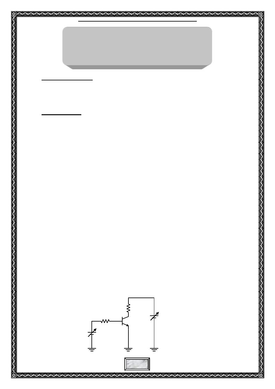
Experiment No. (4)
Common Emitter Biasing Circuit
R
B
V
BB
R
C
V
CC
Fig. 1
Experiment (4): Common Emitter Amplification Circuit
2
2016-2017
Fig. 2: The DC Load Line
Effect of AC input signal on the dc load line: Assume a sinusoidal voltage,
V
IN
, is superimposed on V
BB
(Fig. 3), causing I
B
current to vary sinusoidally
above and below Q-point. This, in turn, causes the I
C
and V
CE
to vary above
and below its Q-point. If the Q-point driven into saturation region, the positive
edge of output voltage clipped by saturation. If the Q-point driven into cut-off
region, the negative edge of output voltage clipped by cut-off.
R
B
V
BB
R
C
V
CC
V
in
Fig. 3
(ii) Transistor Bias Circuits:
(1) Fixed Bias Circuit
In fig. 4(a), A separate DC source, V
BB
, was used to bias base-
emitter junction because it could be varied independently of V
CC
and it
helped to illustrate transistor operation. A more practical bias method
is to use V
CC
as the single bias source as shown in fig. 4(b). this circuit
represent a typical Fixed Bias Circuit.
I
C(mA)
V
CE(V)
I
B
I
B1=0
I
B2
Saturation
Cutoff
I
B3
I
B4
I
B
5
I
B
6
I
B
7
I
B
8
I
B
9
DC Load Line
Q-Point
Vcc
Vcc/R
C
Experiment (4): Common Emitter Amplification Circuit
3
2016-2017
(a)
(b)
Fig. 4: Fixed Bias Circuit
For this circuit (fig. 4(b)):
I
B
= (V
CC
- V
BE
)/ R
B
, I
C
= β I
B
I
C
= β (V
CC
- V
BE
)/ R
B
From last equation, we notice that I
C
is dependent on β, the
disadvantage of this circuit is that a variation in β cause I
C
and, as a
result V
CE
to change, thus changing the Q-point of the transistor, this
make the Fixed bias circuit extremely depend on β and very unstable.
In order to increase the stability of the circuit, the above bias
circuits can be improved to other type of biasing.
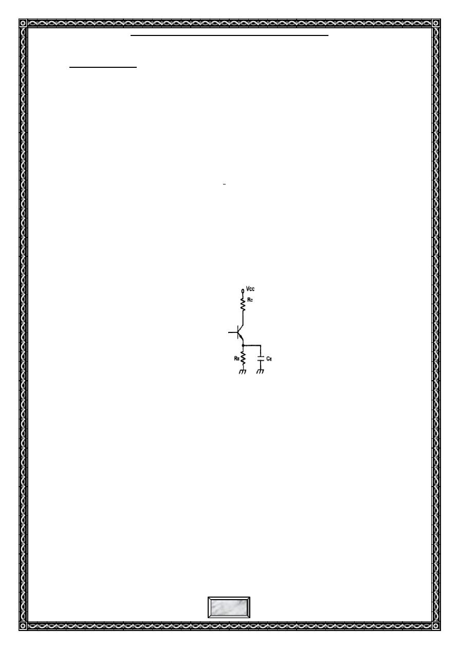
(2) Voltage-Divider Bias Circuit
Fig. 5 shows Voltage Divider Bias circuit, the operation point
for this circuit more stable than fixed bias circuit and not be shifted due
to the difference of β values. As this circuit has the characteristics to
automatically lock its operating point, this circuit is also called "Self-
Bias Circuit".
Fig. 5: Voltage-Divider Bias Circuit
The equivalent circuit of Fig. 5 is shown in Fig. 6
.
Fig. 6
Experiment (4): Common Emitter Amplification Circuit
4
2016-2017
For this circuit (Fig. 6):
V
BB
= I
B
R
BB
+V
BE
+I
E
R
E
Substituting I
E
/β for I
B
and by suppose R
E
>>R
BB
/β, then:
I
E
= (V
BB
-V
BE
)/ R
E
The last equation shows that IE, and therefore IC, is
independent on β (β does not appear in the equation) on the condition
that RE is at least ten times the resistance of the parallel combination
of the voltage divider resistance R
BB
divided by the minimum β.
Voltage divider bias is widely used because reasonably good
stability is achieved with a single supply voltage.
(3) Collector-Feedback Bias Circuit
Collector-Feedback Bias circuit is shown in Fig. 7. the
negative feedback creates an "offsetting" effect that tends to keep Q-
point stable. If I
C
tried to increase, it drops more voltage across R
C
,
thereby causing V
CE
to decrease. When V
CE
decrease, there is decrease
in voltage across R
B
, which decrease I
B
. the decrease in I
B
produce less
I
C
which, in turn, drops less voltage across R
C
and thus offsets the
decrease in V
CE
.
Fig. 7: Collector-feedback Bias Circuit
Among different β values, the locations of the operating points
are not obviously different. Comparing with fixed bias circuit the
collector-feedback bias circuit is significantly stable. As this circuit
will function as automatically adjusted, I
C
will not be significantly
changed due to the variation of β value.
Summary:
1. Fixed Bias circuit arrangement has poor stability because its Q-point
varies widely with β.
2. Voltage Divider bias provides good Q-point stability with a single
polarity supply voltage. It’s the most common bias circuit.
3. Collector-Feedback bias provides good stability using negative
feedback from collector to base.
Experiment (4): Common Emitter Amplification Circuit
5
2016-2017
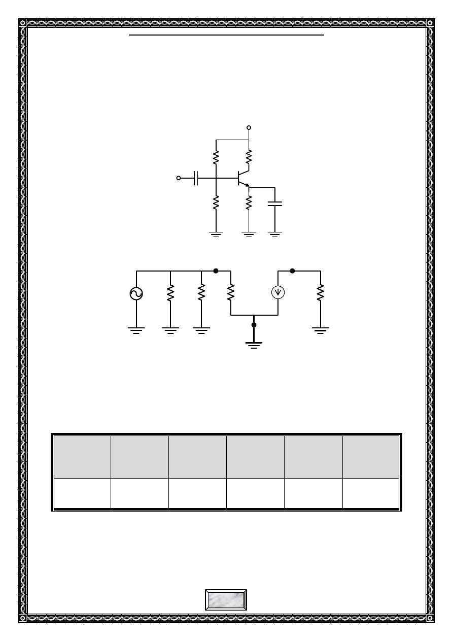
iii) AC circuit analysis for CE amplifier
The common-emitter amplifier is characterized by high voltage (A
v
)
and current gain (A
i
). The amplifier typically has a (1 to 10 kΩ) input
resistance and is generally used to drive medium to high resistance loads.
For the voltage divider CE amplifier circuit is shown in Fig. 8, and its
equivalent is shown in Fig. 9.
Fig. 8
Fig. 9
Table-1 shows the Characteristic of CE Amplifier.
Table-1: CE Amplifier Characteristic
Voltage
Gain
A
V
Current
Gain
A
i
Power
Gain
A
p
Input
Resistance
R
in
Output
Resistance
R
o
Relation
between
input/output
phase
High
(-R
c
/r
e
)
High
(β)
Very High
(A
V
A
i
)
Medium
(βr
e
)
Medium
/
c
r
180°
βre
βib
V
in
R
1
R
2
R
C
E
B
C
R
C
R
2
R
1
c
i
R
E
c
E
V
CC
V
in
Experiment (4): Common Emitter Amplification Circuit
6
2016-2017
Experiment Equipments:
(1) KL-200 Linear Circuit Lab.
(2) Experiment Module: KL-23003.
(3) Experiment Instrument: 1. Multimeter or digital multimeter.
2. Oscilloscope.
(4) Tools: Basic hand tools.
(5) Materials: As indicated in the KL-23003.
Experiment Items:
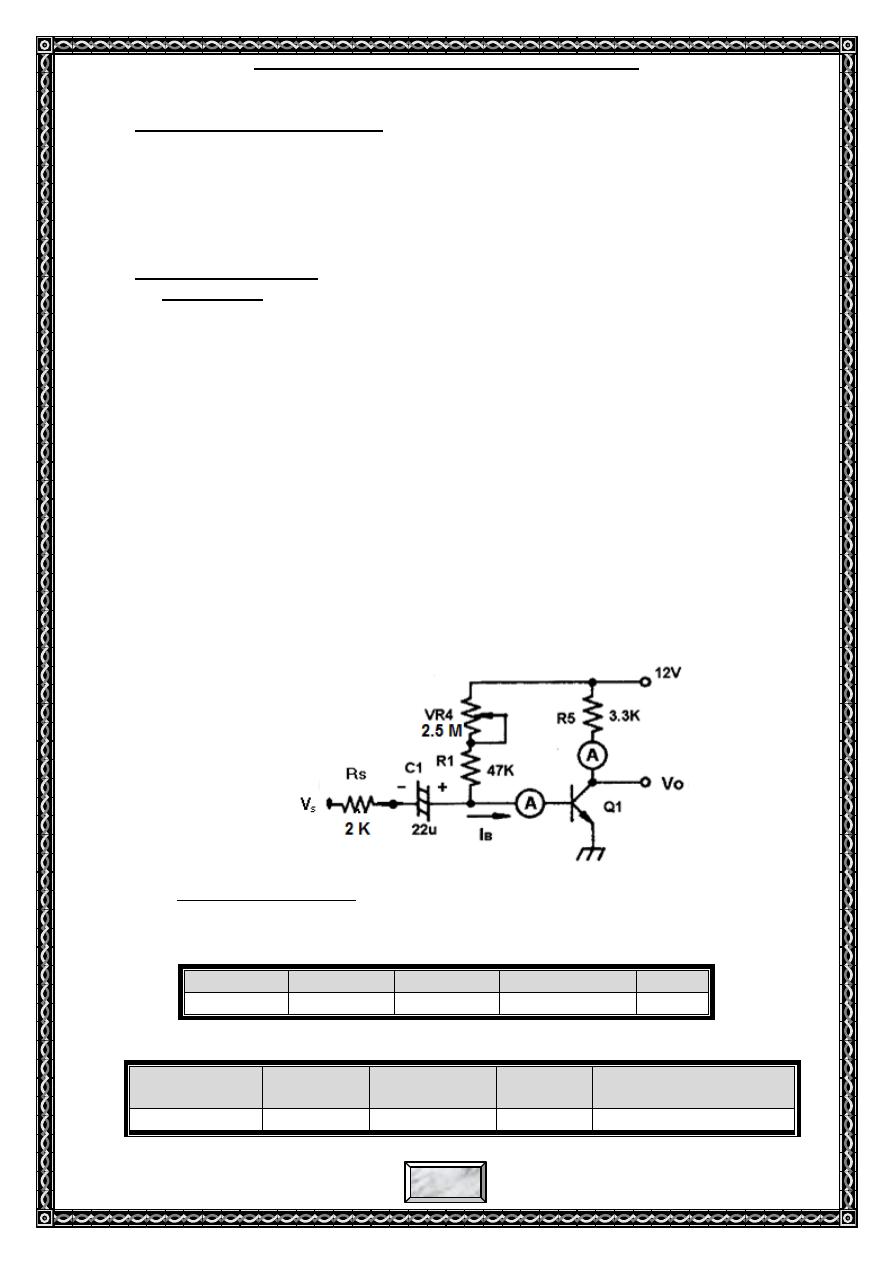
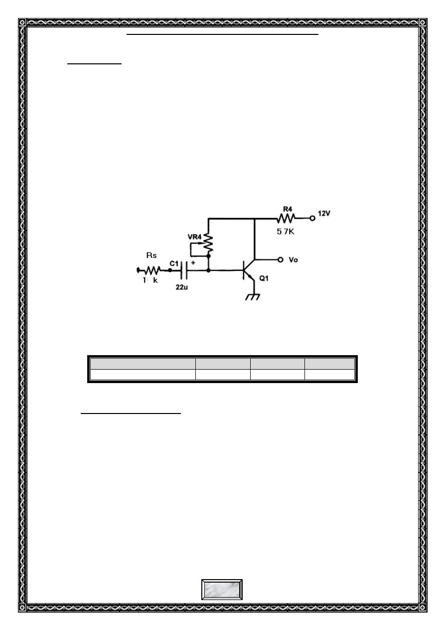
Item one (1): Experiment Procedures for Fixed Bias
(1) Connect the circuit shown as Fig. 10, connect to the DC +12V. Don’t
connect AC signal at input (Vs) .
(2) Adjust VR4, so that V
CE
= 1/2V
CC
, then record V
BE
, I
B
and I
C ,
as shown in
table 2-a below.
(3) Connect signal generator(Vs) to the input terminal Vs and connect channel
one of oscilloscope (AC position) to the input and the other channel to the
output terminal V
o
, then adjust signal generator so that the oscilloscope
can display maximum non-distorted waveform of 1kHz sine wave( apply
Vs = 10mV,20 mV,30 mV,40 mV,50 mV,60 mV, 70 mV,80 mV, 90 mV,
100 mV,175mV). see the output (Vo) at each value.
(4) When the maximum non-distorted waveform is generated in V
o
, use
oscilloscope to measure and draw input and output signal, as table(2-b).
(5) Remain the input signal(Vs) unchanged and adjust VR4 (2.5MΩ), then view
if you notice the output waveform distorted or no, if output waveform is
distorted why write? .Draw Vo and Vi at V
CE
= 3, and then at V
CE
= 9 V
(adjust VR4 to get 3 and 6V).
Experiment Results :
(a) Recorded in Table -2.
(b) Draw V
op-p
and V
ip-p
with respect to time.
Table -2: (a) DC results
(b) AC results
V
CE
V
BE
I
C
(mA)
I
B
(µA)
β
6 V
V
CE
(DC)
V
o
V
in
A
v
Phase shift between
Vs and Vo
6 V
Fig. 10
Experiment (4): Common Emitter Amplification Circuit
7
2016-2017
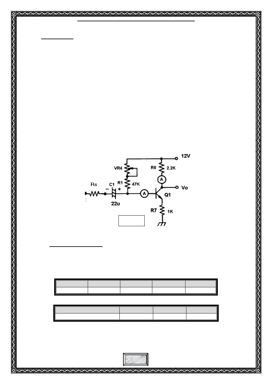
Item Two (2): Experiment Procedures for Emitter Self Bias
(1) Connect the circuit shown as Fig. 11, connect to the DC +12V, Don’t
connect AC signal at input (Vs) .
(2) Adjust VR4, so that V
CE
= 1/2V
CC
, then record V
BE
, I
B
and I
C
as shown in
Table 3-a below .
(3) Connect signal generator(Vs) to the input terminal Vs and connect channel
one of oscilloscope (AC position) to the input and the other channel to the
output terminal V
o
, then adjust signal generator so that the oscilloscope
can display maximum non-distorted waveform of 1kHz sine wave( apply
Vs = 0.5V,0.75V,1V,1.5V,2V,2.5V). see the output (Vo) at each value.
(4) When the maximum non-distorted waveform is generated in Vo, use
oscilloscope to measure input and output signal, as shown in table(3-b) ,
draw V
in
and V
O
at V
CE
(6V) only
.
(5) Remain the input signal(Vs) unchanged and adjust VR4 (2.5MΩ), then view
if you notice the output waveform distorted or no, if output waveform is
distorted why write? .Draw Vo and Vi at V
CE
= 3, and then at V
CE
= 9 V
(adjust VR4 to get 3 and 6V).
Experiment Results:
(a) Record the value of I
B
, I
C
and V
BE
in Table -3.
(b) Draw V
Op-p
and V
ip-p
with respect to time.
Table -3:
(a) DC results
(b) AC results
V
CE
V
BE
I
C(mA)
I
B(uA)
β
6 V
V
CE
(DC)
V
o
V
in
A
v
6V
V
in
V
s
20 k
2.5 M
Fig. 11
Experiment (4): Common Emitter Amplification Circuit
8
2016-2017
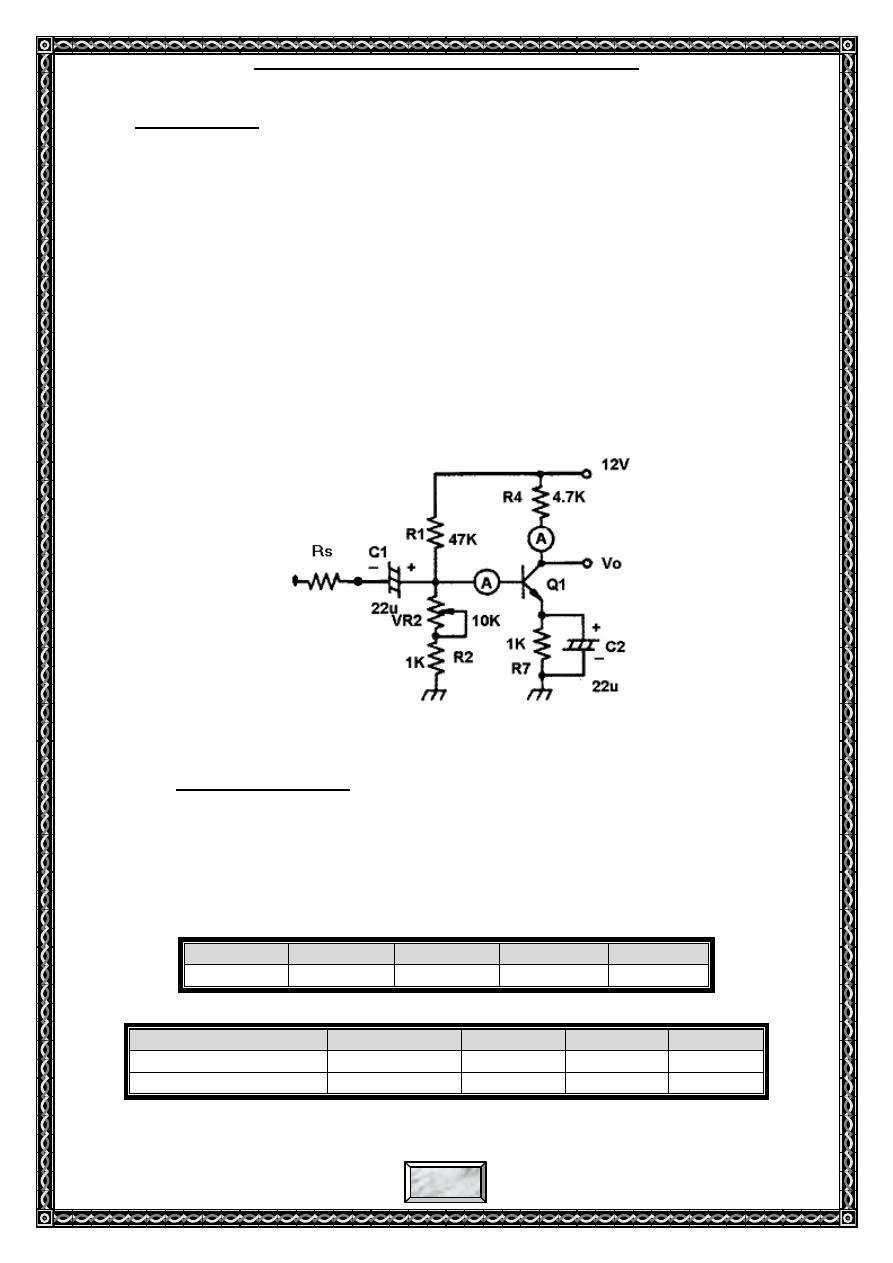
Item Three (3): Experiment Procedures for Voltage-Divider Bias
(1) Connect the circuit shown as in Fig. 12, connect to the DC +12V, Don’t
connect AC signal at input (Vs) .
(2) Adjust VR2 (10kΩ) so that V
CE
= 1/2V
CC
, then view and record the values
of V
BE
, I
B
and I
C
as in table (4-a)..
(3) Connect signal generator to the input terminal (Vs) and connect oscilloscope
to the output terminal (Vo), then adjust 1kHz sine wave of the signal
generator( apply Vs = 50mV,100 mV,150 mV,200 mV,300 mV,4V, 5V).
see the output (Vo) at each value. so that the oscilloscope can display
maximum non-distorted waveform of output then use oscilloscope to
measure input and output signal, as in table (4-b).
(4) Remain the input signal unchanged and adjust VR2 (10kΩ), then view if
the output waveform is distorted.
(5) Disconnect C
2
(22μF), then repeat Step (2) (3) (4).
Fig. 12
Experiment Results:
(a) Record the value of I
B
, I
C
, and V
BE
in table -4 at which C
2
is exist and not
exist. Then calculate the value A
V
= V
Op-p
/ V
ip-p
and the value of β=
I
C
/I
B
.
(b) Draw V
Op-p
and V
ip-p
with respect to time, which C
2
is exist and not exist.
Table -4:
(a) DC results
(b) AC results
V
CE
V
BE
I
C
I
B
β
6 V
V
CE
(DC)
C
2
V
o
V
in
A
v
6 V
Connected
6 V
Disconnected
V
in
V
s
1 K
Experiment (4): Common Emitter Amplification Circuit
9
2016-2017
Item Four (4): Experiment Procedures for Collector-feedback Bias
(1) Connect the circuit shown as in Fig. 13, connect to the DC +12V, Don’t
connect AC signal at input (Vs) .
(2) Adjust VR4 (1MΩ) so that V
CE
= 1/2V
CC
.
(3) Connect signal generator in the input terminal (Vs) and connect
oscilloscope to the output terminal (Vo), then adjust 1kHz sine wave
output of the signal generator( apply Vs = 10mV,20 mV,30 mV,35
mV,50 mV ,1V, 5V). so that the oscilloscope can display maximum non-
distorted waveform of output then use oscilloscope to measure input and
output signal, as table(5).
(4) Remain the input signal unchanged and adjust VR4 (2.5MΩ), then view if
the output waveform is distorted. If distorted, why?
Fig. 13
Table -5:
AC results
4-2 Experiment Result :
(a) Record the values of V
inp-p
and V
op-p
in table -5 and calculate the value of
A
V
.
(b) Draw V
op-p
and V
ip-p
with respect to time.
V
CE
(DC)
V
o
V
in
A
v
6 V
V
in
V
s
2.5M
m
Experiment (4): Common Emitter Amplification Circuit
10
2016-2017
Discussions:
1. Explain briefly the effect of Q point location.
2. Explain the reason of the phase shift in CE.
3. Explain in which type arrangement of Voltage-Divider bias CE
configurations (with or without emitter capacitor C
E
) have best voltage
gain? (Prove the answer with the experiment results).
4. Choose the correct answer:
(a) The disadvantages of a Fixed bias circuit is that:
1. it is very complex.
2. it is too β dependent.
3. it produces low gain.
(b) For maximum output, the Q-point must be:
1. Near saturation.
2. Near cut-off.
3. midpoint between saturation and cut-off.
(c) As shown in the following Figure, what is the function of R
E
?
1. Stabilize the operating point.
2. To increase A
V
.
3. To increase A
i
.
(d) What is the function of C
E
in the above Figure?
1. Stabilize the DC bias.
2. To increase A
V
.
3. To increase A
i
.
(e) The linear region of the transistor lies between:
1. Saturation and Q-point.
2. Saturation and cut-off.
3. Cut-off and Q-point.
(f) For an amplifier circuit, which one is the most common design?
1. The operating point is set near cutoff point.
2. The operating point is set near saturation point.
3. The operating point is set between cutoff and saturation.
5. Write a conclusion for this experiment.