Experiment (6): Common Collector & Base Amplification Circuit
1
2016/2017
Study Objective:
(1) To compute and measure the basic characteristics of CC & CB amplification.
(2) To distinguish between the CC & CB amplifiers.
Introduction:
1. Common Base (CB) Amplifier
(A) Basic knowledge of CB amplifier
The common-base (CB) amplifier provides high voltage gain with a maximum current
gain of 1. Since it has a low input resistance, the CB amplifier is the most appropriate type
for certain application when source tend to have very low-resistance outputs such as
Antennas and Transmission Lines.
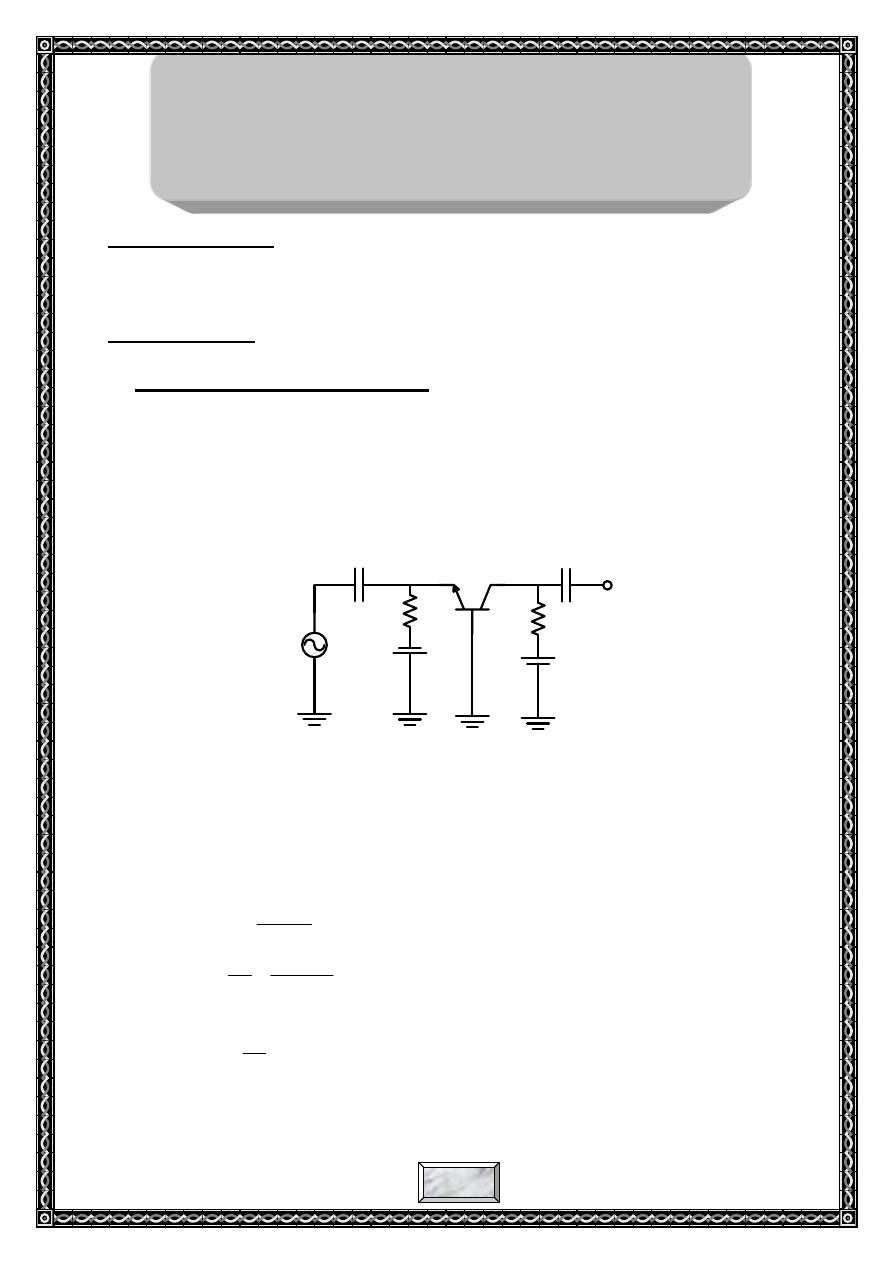
The basic circuit of CB amplifier is shown in Figure (1). As the base is the common
terminal between the V
i
and V
O
. this circuit is thus called common-base (CB) amplifier.
R
E
c
i
R
C
V
in
V
EE
V
CC
c
c
V
o
Figure (1)
(B) DC bias design for CB amplifier
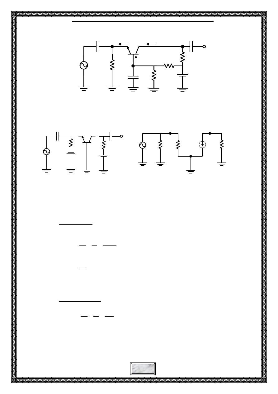
Since the above Figure has two DC power supplies( VCC and VEE ), it is more
practical use the circuit in Figure (2) which is has one DC power supply(VCC). The
base is viewed as short-circuit for AC signal. The base thus seems to be grounded for V
i
and V
O
.
The DC bias is analyzed as follows:
2
1
2
R
R
R
V
V
CC
B
E
BE
B
E
E
E
R
V
V
R
V
I
C
C
CC
C
E
E
C
E
C
R
I
V
V
R
V
I
I
I
Experiment No. (6)
Common Collector & Common Base
Amplifier Circuits
Experiment (6): Common Collector & Base Amplification Circuit
2
2016/2017
R
E
C
1
R
C
V
in
C
2
R
1
R
2
V
o
V
CC
C
B
V
E
V
c
V
B
I
C
I
E
I
B
Figure (2)
(C) AC analysis for CB amplifier
The circuit shown in Figure (3a) can be represented by the equivalent circuit of
Figure (3b).
(a)
(b)
Figure (3)
From this circuit we can find out that the CB amplifier has the following
characteristics:
1. Voltage Gain:
The voltage gain from emitter to collector is developed as follows (V
in
=v
e
,
V
o
=v
c
)
e
e
C
e
e
c
in
o
v
r
i
R
i
v
v
V
V
A
since
1
, then:
e
C
v
r
R
A
Notice that the given expression is the same for the CE amplifier. However,
there is no phase inversion from emitter to collector in CB.
2. Input Resistance:
The resistance appears at the emitter (input) is:
e
e
e
e
e
in
in
in
i
r
i
i
v
I
V
R
e
in
r
R
Since the input resistance of CB amplifier (
e
r
) is depends on the input current, ie,
c
e
I
mv
r
/
26
R
E
c
i
R
C
V
in
V
EE
V
CC
c
o
V
in
R
E
r
e
B
E
C
R
C
V
o
αi
e
Experiment (6): Common Collector & Base Amplification Circuit
3
2016/2017
the large input signal suffers from distortion greater than the small signal. This is the
reason that CB amplifier operates only on the small signal and known as a small signal
amplifier
3. Output Resistance:
Looking into the collector (output), the output resister is simply the collector
resistor:
C
o
R
R
4. Current Gain:
The current gain is the output current divided by the input current. i
c
is the ac
output current, and i
e
is the ac input current. Since
e
c
i
i
, the current gain is
approximately 1.
1
i
A
2. Common Collector (CC) Amplifier
(A) Basic knowledge of CC amplifier
Common-collector (CC) or emitter follower amplifier is an important small signal
amplifier configuration. It is very useful one because it has very high input resistance,
high current gain, very small output resistance, and approximately unity voltage gain.
The high input resistance and low output resistance make the emitter follower an ideal
buffer between a high impedance source and a low impedance load. A buffer is any
circuit that keeps the source from being affected by a load.
CC amplifier is shown in Figure(4), you can seen that the input is from the base
and the output from emitter as well as the V
CC
will be short-circuit with respect to AC
signal (in the equivalent circuit), C is the common terminal between V
in
and V
o
. In
other words, C is grounded
.
R
B
c
in
R
E
c
E
V
CC
V
in
V
o
R
B
R
E
V
CC
V
E
I
B
I
C
I
E
V
BE
Figure(4)
Figure(5)
(B) DC bias design for CC amplifier
The emitter-feedback bias circuit is shown in Fig. 2. where
E
B
R
I
)
1
(
V
R
I
R
I
V
R
I
V
BE
B
B
E
E
BE
B
B
CC
E
B
BE
CC
B
R
R
V
V
I
)
1
(
B
B
I
I
)
(1
I
I
I
C
B
E
and
E
E
E
R
I
V
Experiment (6): Common Collector & Base Amplification Circuit
4
2016/2017
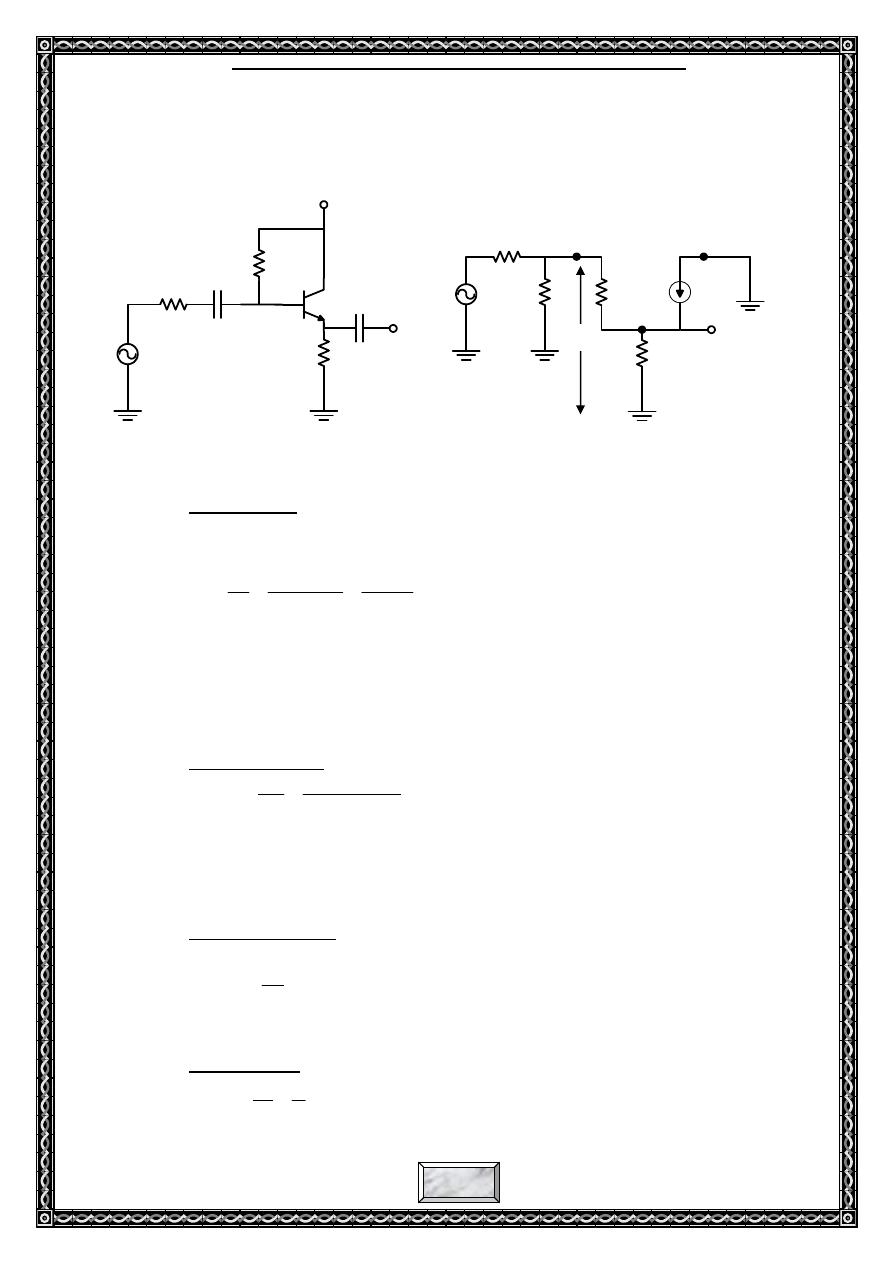
(C) AC analysis for CC amplifier
The following small-signal AC equivalent circuit (Figure(6b)) can be used to
calculate the voltage gain, input resistance, and output resistance of the common-
collector amplifier of Figure(6a).
(a)
(b)
Figure (6)
1. Voltage Gain:
)
(
E
e
e
in
E
e
o
R
r
i
V
R
i
V
E
e
E
E
e
e
E
e
in
o
v
R
r
R
R
r
i
R
i
V
V
A
)
(
If R
E
>>r
e
, then a good approximation is:
1
v
A
Since the output voltage is at the emitter, it is in phase with the base voltage, so there
is no inversion from input to output. Because there is no inversion and because
the voltage gain is approximately 1, the output voltage closely follows the input
voltage in both phase and amplitude; thus the term Emitter-follower.
2. Input Resistance:
b
E
b
e
b
in
in
in
i
R
i
r
i
I
V
R
)
(
E
e
in
R
r
R
If R
E
>>r
e,
then:
E
in
R
R
3. Output Resistance:
The output resistance, looking into emitter of CC, is approximated as follows:
e
E
e
S
o
r
R
r
R
R
\
\
)
(
Where R
S
is the resistance of input source.
4. Current Gain:
b
e
i
i
i
I
I
A
in
o
R
B
c
i
R
E
c
E
V
CC
V
S
V
o
R
S
V
s
R
B
re
ßib
E
B
C
R
E
V
o
R
s
βr
e
βi
b
V
in
Experiment (6): Common Collector & Base Amplification Circuit
5
2016/2017
CC amplifier is not applicable in voltage amplification, but is suitable for
impedance
matching.
Common-emitter, Common-collector, and Common-base amplifier configuration
are summarized in Table -1.
Table -1: Relative Comparison of Amplifier Configurations
CE
CC
CB
Voltage Gain, A
V
High
R
c
/r
e
Low
≈1
High
R
c
/r
e
Current Gain, A
i
High
β
High
β
Low
≈1
Power Gain, A
p
Very High
A
i
A
v
High
≈A
i
High
≈A
v
Input Resistance, R
in
Low
βr
e
High
βR
E
Very Low
r
e
Stage Output
Resistance, R
o
High
/
c
r
Very Low
e
r
High
c
r
Phase Angle
180
o
0
o
0
o
Experiment (6): Common Collector & Base Amplification Circuit
6
2016/2017
Experiment Equipments:
(1) KL-200 Linear Circuit Lab.
(2) Experiment Module: KL-23003.
(3) Experiment Instrument: 1. Multimeter or digital multimeter.
2.Two channel Oscilloscope.
(4) Materials: As indicated in the KL-23003.
Experiment Items:
Item One (1) Experiment for CB amplifier.
Experiment Procedures:
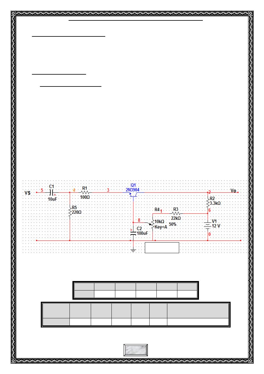
(1) Insert the short-circuit clips by referring to Figure(7), Connect the DC +12V without
connecting input signal (Use transistor 2N3904 ).
(2) Adjust VR2 (10kΩ), so that V
CB
= 1/2V
CC
, then record V
BE
,
I
E,
I
B
and I
C
as shown in
table (2a)
(3) Connect signal generator to the input terminal V
in
(IN) and (Channel 1) oscilloscope
(DC position. Then connect (Channel 2) oscilloscope (DC position) to the output
terminal V
o
(OUT).
(4) Adjust the signal generator frequency to l kHz and Then adjust signal generator such
that the oscilloscope can display maximum non-distorted output view V
in
and V
o ,
( apply Vs = 300mV
P-P
,350 mV
P-P
,400 mV
P-P
,410 mV
P-P
,420 mV
P-P
,450 mV
P-P
, 500
mV
P-P
,800 mV
P-P
). see the output (Vo) at each value.
(5) Use oscilloscope to measure v
in
, v
a
and v
o
respectively, then calculate A
v
as shown in
table (2b)
(6) Move the Q point location up and down till the output is distorted and sketch the
output in each case .
Table -2:
(a) DC results
(b) AC results
V
CB
V
BE
I
B
I
E
I
C
β
6V
V
CB
(DC)
v
S (p-p)
V
a(p-p)
v
in
(p-p)
v
o(p-p)
A
v
Phase shift between
Vi and Vo
6V
Figure(7)
Va
Vi
Experiment (6): Common Collector & Base Amplification Circuit
7
2016/2017
Item Two (2): Experiment for CC amplifier
Experiment Procedures:
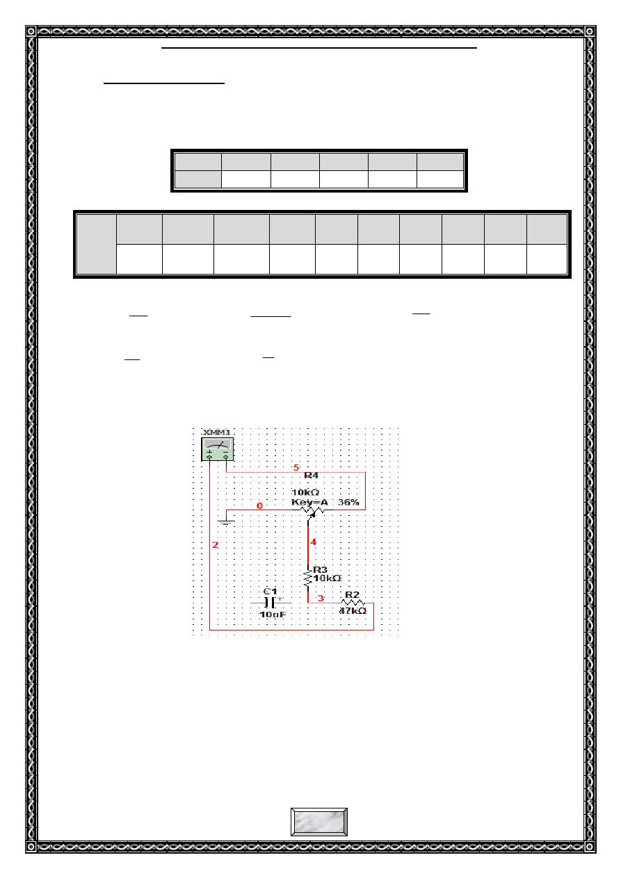
(1) Insert the short-circuit clips by referring to Figure(8), Connect the DC +12V without
connecting input signal (Use transistor 2N3904).
(2) Adjust VR2 (10kΩ), so that V
CE
= 1/2V
CC
, then record V
BE
, I
B
and I
C
as shown in
table (3 )
(3) Connect signal generator to the input terminal V
in
(IN) and (Channel 1) oscilloscope
(DC position. Then connect (Channel 2) oscilloscope (DC position) to the output
terminal V
o
(OUT). Then adjust signal generator such that the oscilloscope can
display
maximum
non-distorted
output,
(
apply
Vs
=
2V
P-P
,4V
P-P
,
8 V
P-P
,9V
P-P
,10V
P-P
,12V
P-P
, 20V
P-P
). see the output (Vo) at each value. Sketch V
in
and V
o
at maximum non-distorted output voltage.
(4) Use the oscilloscope to measure
v
a
(p-p)
,
v
in
(p-p)
and
v
o(p-p)
as in table (3b)
(5) Move the Q point location up and down till the output is distorted and sketch the
output in each case
Experiment (6): Common Collector & Base Amplification Circuit
8
2016/2017
Experiment Results:
(a)Tabulate your results as shown in Table (3a,b).
(b)Graphs of steps 3 and 5.
Table -3:
(a) DC results
(b) AC results
E
e
R
v
i
O
,
B
b
R
v
v
i
in
a
,
b
in
i
v
R
in
,
in
v
v
A
O
V
,
b
i
i
A
e
i
,
i
V
P
A
A
A
.
V
CE
V
BE
I
B
I
E
I
C
β
6V
VCE
= 6V
V
S
(p-p)
v
a
(p-p)
v
in
(p-p)
v
o(p-p)
i
e(p-p)
i
b(p-p)
R
in
A
v
A
i
A
p

Experiment (6): Common Collector & Base Amplification Circuit
9
2016/2017
Discussion:
1. Why the buffer is used to match between high resistance source and low resistance
load?. Explain why we can use CC as a buffer.
2. Explain why the CB known as small signal amplifier?
3. Match the following generalized characteristic with the appropriate (C.E, C.B, C.C)
amplifier configuration:
a. Good current gain, unity voltage gain, high input resistance.
b. Good current gain, good voltage gain, low input resistance.
c. Unity current gain, good voltage gain, low input resistance.
4. Explain why the CC amplifier is called Emitter-follower?.
5. Choose the correct answer:
(a) A small signal Amplifier
1. Goes into saturation once on each input cycle.
2. Uses only a small portion of its load line.
3. Is always a common-emitter amplifier.
(b) Among all configurations of the transistor amplifiers, which one has the largest of
voltage gain and current gain?
1. CE configuration.
2. CC configuration.
3. CB configuration.
(c) In a certain emitter-follower circuit, the current gain is 50. The power gain is
1. 50 AV.
2. 50.
3. Answers 1 and 2.
(d) The main disadvantage of the CB amplifier compared to the CE and CC amplifier
1. has low input resistance.
2. its power gain ≈A
V
.
3. has low current gain.
(e) If one stage of CC amplifier is connected between two stages of CE amplifiers,
what is the function of this CC amplifier?
1. Voltage amplification.
2. Impedance matching.
3. Current amplification.
6. Writ a conclusion for this experiment.